
Acidic ammonothermal growth promises cheaper GaN
Acidic ammonothermal growth can be carried out at relatively low pressures, allowing the use of larger autoclaves with a higher throughput
Devising a great process for the commercial production of GaN substrates is far from easy. The incumbent technology, HVPE, delivers reasonable throughout at the expense of material quality, while the primary alternative, ammonothermal growth, majors on high crystal quality, but is impaired by a low throughout that drives up production costs. However, the limitations of ammonothermal growth could soon be addressed, thanks to a team from Japan that has boosted throughput with larger autoclaves employing acidic mineralisers.
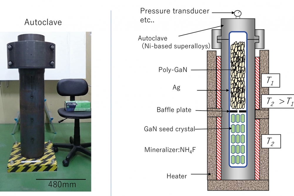
Conventional ammonothermal growth uses basic mineralisers and temperatures of more than 600 °C. Growth takes place in autoclaves made from nickel-based superalloys that have a high strength at elevated temperatures, but the high pressures required for crystal formation restricts the size of the growth reactor.
Switching from basic mineralisers to those that are acidic allows lower growth pressures, and thus larger autoclaves that provide a higher throughput.
The Japanese collaboration that’s exploring this opportunity brings together researchers from Tohoku University, Mitsubishi Chemical Corporation and The Japan Steel Works, which has a great deal of expertise in producing autoclaves. This company has made more than 400 of them for the production of quartz via the hydrothermal method, and can draw on 15 years of research-based experience when producing autoclaves for basic ammonothermal growth of GaN.
Team spokesman Shigefusa Chichibu claims that they are the first to report the growth of large, flat, c-plane GaN using a low-pressure acidic ammonothermal process. He added: “This uses half the pressure of conventional acidic ammonothermal methods and a quarter of basic ammonothermal methods.”
The team carried out GaN growth in an autoclave capable of accommodating crystals up to 4 inches in diameter. This vessel is lined with silver to prevent corrosion from a reaction between supercritical ammonia and acid.
GaN seeds were placed in the bottom half of the autoclave, where the temperature is higher. Above them, where it is cooler, the team added polycrystalline GaN, the raw material. This particular arrangement aided the growth of high-quality GaN, because the higher temperature where crystal growth occurs supressed the generation of point defects, and impurity atoms were transported to the low-temperature zone.
The researchers have studied GaN material formed after 21 days of growth on: a 2-inch diameter, HVPE-grown seed; and a 10 mm by 10 mm seed, produced by the acidic ammonothermal method. GaN grown on the HVPE seed suffered from tilt and twist mosaics, while that formed on the ammonothermal seed yielded a 3 mm-thick smooth, flat GaN crystal.
Informed by their finding, Chichibu and co-workers inserted a 60 mm by 60 mm seed produced by the ammonothermal method into the autoclave. 14 days of growth produced a 3 mm-thick, smooth, flat GaN crystal. It is almost bow free, and when assessed by X-ray diffraction, produces a peak with a full-width at half-maximum of just 13 arcsec.
Since reporting these results, the team has installed a much larger autoclave. “We are currently conducting growth experiments for 4-inch and 6-inch mass production,” revealed Chichibu, who added that the next goals for the team are to produce GaN substrates grown by low-pressure acidic ammonothermal growth for customers, and to accelerate device evaluation.
REFERENCE
K. Kurimoto et al. Appl. Phys. Express 15 055504 (2022)


