Loading...
News Article

Plasma-Therm Rolls Out Redesigned Heatpulse Platform

News

Re-engineered for demands of power devices, GaAs, GaN and SiC and ≤200mm silicon wafers

Plasma-Therm has redesigned its flagship Heatpulse Rapid Thermal Processing (RTP) platform. The move was driven by an increase in market demand for power devices, other specialty markets and ≤200mm silicon fabs.

Representing the first of several phases in Plasma-Therm’s planned technology roadmap for Heatpulse RTP, the new platform includes greater flexibility to accommodate multiple wafer sizes, upgraded robotics, and a control system backed by Cortex, Plasma-Therm’s software.

By using readily available components instead of specialised custom parts to maintain their equipment, customers can mitigate supply chain and replacement parts challenges to optimise production yields and capacity with maximise uptime during high-volume manufacturing. Additionally, the new easily implemented Heatpulse RTP wafer size conversion kits eliminate the complicated, time-consuming system hardware changes.

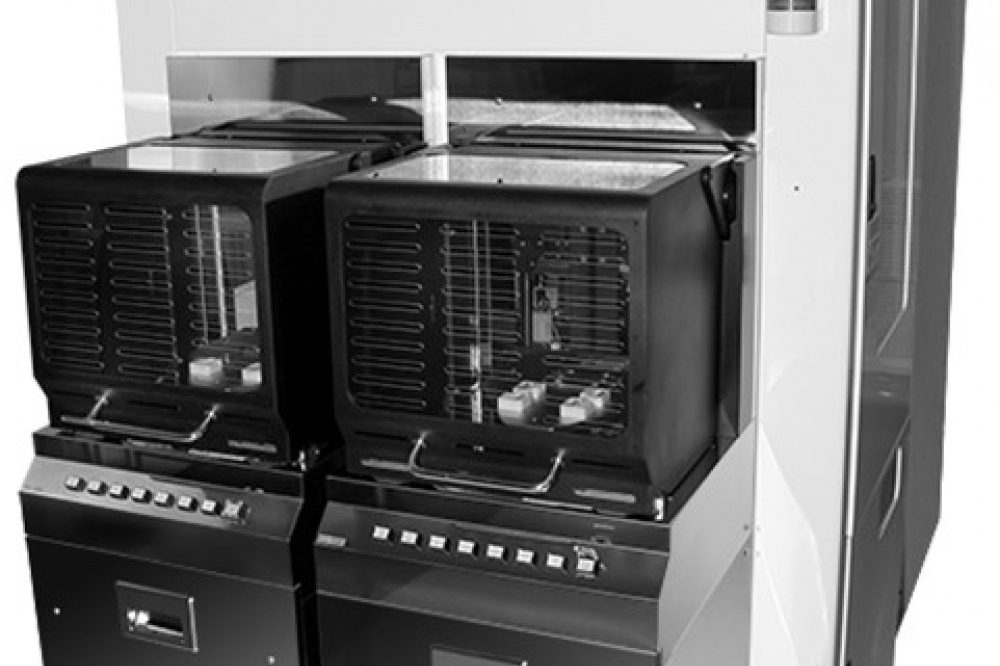
Like its predecessor Heatpulse 8800 and 8108 models, the new Plasma-Therm Heatpulse RTP platform can process substrates up to 200mm in diameter and can handle a diverse range of materials. This includes traditional CMOS silicon as well as compound semiconductors, such as GaAs, GaN and SiC.

The Heatpulse technology features are designed to address a multitude of semiconductor process steps, including post-implant annealing, oxide and nitride film growth, reflow, and formation of silicides, salicides, metal alloys, as well as ohmic contact formation. The Heatpulse RTP is available in either a single-oven or a new dual-oven configuration unique to the redesigned platform, and features a multi-zoned, independently controlled temperature capability.

SPONSOR MESSAGE

Secure Your Hydrogen Supply

A study supply of high-purity hydrogen is critical to semiconductor fabrication. Supply chain interruptions are challenging manufacturers, leading to production slowdowns and stoppages. On-site hydrogen generation offers a scalable alternative for new and existing fabs, freeing the operator from dependence on delivered gas.

Plant managers understand the critical role that hydrogen plays in semiconductor fabrication. That important job includes crystal growth, carrier gas, wafer annealing, and in the emerging Extreme UV Lithography (EUV) that will enable new generations of devices. As the vast need for semiconductors grows across all sectors of world economies, so does the need for high-purity hydrogen.

Take control with Nel on-site hydrogen generation.

Read more
QD company Quantum Science expands into new facility
Innoscience files lawsuit against Infineon
Riber revenues up 5% to €41.2m
Forvia Hella to use CoolSiC for next generation charging
Photon Design to exhibit QD simulation tool
Ortel transfers CW laser fabrication to Canada
Luminus adds red and blue multi-mode Lasers
PseudolithIC raises $6M for heterogeneous chiplet tech
Mesa sidewall design improves HV DUV LEDs
IQE revenue to exceed expectations
'Game-changing' VCSEL system targets clinical imaging
German start-up secures finance for SiC processing tech
Macom signs preliminaries for CHIPS Act funding
IQE and Quintessent partner on QD lasers for AI
EU funds perovskite tandems for fuel-free space propulsion
EU to invest €3m in GeSi quantum project
Transforming the current density of AlN Schottky barrier diodes
Turbocharging the GaN MOSFET with a HfO₂ gate
Wolfspeed launches Gen 4 SiC MOSFET technology
Report predicts high growth for UK's North East
Element Six unveils Cu-diamond composite
SemiQ launches hi-rel 1700V SiC MOSFETs
Lynred to exhibit Eyesential SWIR sensor for machine vision
Thorlabs buys VCSEL firm Praevium Research
Advancing tuneable InP lasers on a heterogeneous platform
P-GaN gate HEMTs have record threshold voltage
Guerrilla RF releases GaN power amplifier dice
Narrow-linewidth DFB lasers now at 405 and 488nm
Researchers develop tech for future fast-charging stations
Vermont GaN Tech Hub awarded nearly $24M
Onsemi completes buy-out of Qorvo SiC JFET business
Quantum Science announces Innovate UK funding
×
Search the news archive

To close this popup you can press escape or click the close icon.
Logo
x
Logo
×
Register - Step 1

You may choose to subscribe to the Compound Semiconductor Magazine, the Compound Semiconductor Newsletter, or both. You may also request additional information if required, before submitting your application.


Please subscribe me to:


You chose the industry type of "Other"

Please enter the industry that you work in:
 
x
Adblocker Detected
Please consider unblocking adverts on this website