
EVG achieves die-to-wafer fusion and hybrid bonding.
Successful full-system die-to-wafer transfer demonstrates important step forward in achieving process maturity
Wafer bonding and lithography specialist EVG has achieved a breakthrough in die-to-wafer (D2W) fusion and hybrid bonding.
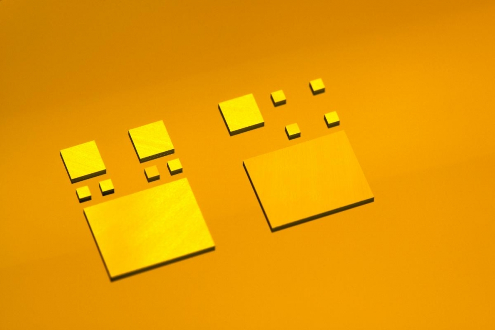
It has successfully demonstrated 100-percent void-free bonding yield of multiple die of different sizes use from a complete 3D system-on-a-chip (SoC) in a single transfer process using EVG’s GEMINI FB automated hybrid bonding system.
Such an accomplishment had been a key challenge for D2W bonding until today, as well as a major hurdle to scaling down the cost of implementing heterogeneous integration. This important industry achievement was carried out at EVG’s Heterogeneous Integration Competence Center (HICC), which is designed to assist customers in leveraging EVG’s process solutions and expertise to accelerate the development of new and differentiating products and applications driven by advances in system integration and packaging.
Company executives will be available to discuss this D2W bonding breakthrough at SEMICON West, taking place this week at the Moscone Center in San Francisco, Calif., from July 12-14.
Applications such as artificial intelligence (AI), autonomous driving, augmented/virtual reality and 5G all require the development of high-bandwidth, high-performance and low-power-consumption devices without increasing production cost.
As a result, the semiconductor industry is turning to heterogeneous integration – the manufacturing, assembly and packaging of multiple different components or dies with different feature sizes and materials onto a single device or package -- in order to increase performance on new device generations. D2W hybrid bonding is a key manufacturing technology for heterogeneous integration. Yet, as the ever-higher bandwidth needs of these devices drive newer packaging technologies, new developments in D2W hybrid bonding and metrology are also needed.
“Hybrid bonding requires substantially different manufacturing technologies to standard packaging processes, bringing it much closer to front-end manufacturing - especially in terms of cleanliness, particle control, alignment and metrology precision,” stated Thomas Uhrmann, business development director at EV Group.
"Between our established GEMINI FB, which has been configured for collective D2W integration flows and serving the needs for D2W bonding for several years already, the EVG 320 D2W die preparation and activation system for direct placement D2W bonding, which provides a direct interface with D2W bonders, and the EVG 40 NT2 overlay metrology system, which uses AI, feed-forward and feedback loops to further increase hybrid bonding yields, EVG provides a complete end-to-end hybrid bonding solution to accelerate the deployment of 3D/heterogeneous integration.”
Since the interface in hybrid bonding is solid-state, with embedded metal pads to allow for face-to-face electrical connection of wafers and dies, D2W hybrid bonding requires similar tight cleanliness standards and manufacturing tolerances seen in front-end semiconductor manufacturing processes. This trend is also moving high-precision metrology into a more central role in controlling hybrid bonding alignment and process yield, which in turn is driving the integration of D2W bonding and metrology processes into one process line.
In addition, several different D2W hybrid bonding process flows are under evaluation today, each with unique advantages and requirements.
Since its establishment two years ago, EVG’s HICC has played a key role in helping customers and partners develop and optimise D2W hybrid bonding processes to address the unique needs of their given device design and application, taking into account various factors such as die size, die thickness, total stack height as well as interface considerations such as contact design and density. The HICC also features a state-of-the-art cleanroom with cleanliness standards on par with many leading-edge semiconductor fabs -- enabling EVG to uniquely support the stringent requirements for D2W and W2W hybrid bonding process development.
"The HICC has firmly established itself as a preeminent central open-access incubator for novel process solutions such as D2W hybrid and fusion bonding,” stated Markus Wimplinger, corporate technology development and IP director at EV Group.


