
LPE and A*STAR IME to collaborate on SiC
Partners to leverage LPE’s knowhow in SiC CVD reactors and epitaxial growth using IME’s research facilities
LPE and Singapore's Institute of Microelectronics (IME) at the Agency for Science, Technology and Research (A*STAR) have announced a research collaboration to develop high quality 200mm SiC and specialty epitaxy processes including enhanced growth rates with improved uniformity. This will be done through experimental activities supported by simulation studies.
Under the collaboration, the parties will leverage LPE’s knowledge in SiC CVD reactor technology and SiC epitaxial growth, plus IME’s research capabilities and facilities, 200mm SiC pilot process integration line, and cutting-edge material characterisation equipment. The aim is to create 200mm epitaxy processes with enhanced growth rate and uniformities, and reduced killer defect densities.
The 200mm SiC pilot line is being established by A*STAR’s IME to validate 200mm manufacturing processes and tools on a pilot scale before transitioning to 200mm high-volume manufacturing. This collaboration will be part of IME’s plans for establishing a 200mm SiC innovation programme.
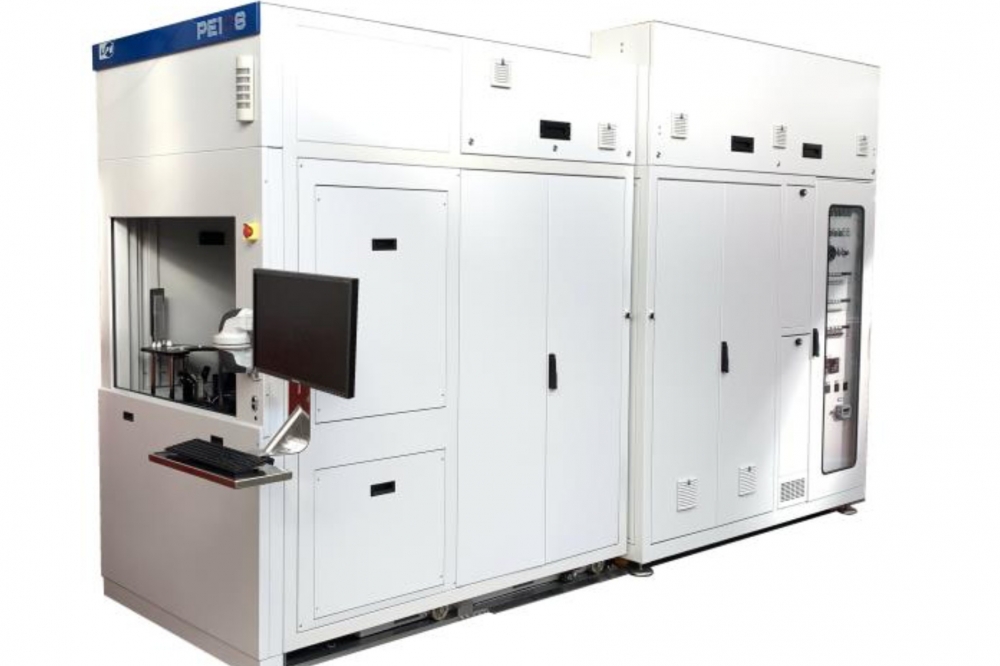
SiC epitaxy is one of the essential process steps for 200mm device processing of the upcoming 200mm SiC pilot line. The manufacturing industry is projected to move towards using a unique single-wafer chamber SiC epitaxy tool. LPE, which contributes their tools into the innovation programme, is geared towards quicker industrial adoption.
For this collaboration, both parties will work on the development of high quality 200mm SiC and specialty epitaxy processes, including the following areas: validation of LPE PE1O8 SiC epitaxy reactor for 150mm / 200mm wafers; rnhancement of 200mm SiC epilayer uniformity; development of 200mm SiC epitaxy processes with increased growth rates; and development of specialty SiC epitaxy processes on 200mm SiC wafers.
“All of us at LPE are very excited about the collaboration with A*STAR's IME which will result in extraordinary market expansion of 200mm SiC based devices. As SiC power modules become pervasive, a more efficient use of electrical power will make a sustainable growth possible,” said Franco Preti, CEO at LPE.
“We look forward to this joint research between A*STAR’s Institute of Microelectronics and LPE to develop high quality 200mm SiC and specialty epitaxy processes,” said Mr Terence Gan, Executive Director, A*STAR’s IME. “The success of this collaboration will benefit the SiC manufacturing ecosystem and accelerate the adoption of high performance SiC power modules across various applications such as electric vehicles and charging points,” he added.


