
Trimming the thermal resistance of Ga2O3 Schottky barrier diodes
Thinning the native substrate leads to a record-breaking power-conversion efficiency
The Achilles heel of the Ga2O3 power device is its poor heat dissipation, attributed to the low thermal conductivity of this oxide. But this weakness can be diminished through substantial thinning of the substrate, leading to a record-breaking power conversion efficiency, according to a team from Nanjing University, China.
Those engineers point out that the body thickness of advanced Ga2O3 devices is typically between 400 mm and 600 mm – but with their three-step process, this is reduced below 100 mm, leading to a cut in thermal resistance for Schottky barrier diodes that then deliver better power characteristics.
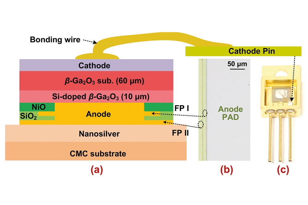
Devices are produced by processing epiwafers made by Novel Crystal Technology, Japan. These epiwafers combine a 640 mm-thick tin-doped b-Ga2O3substrate with a 10 mm-thick silicon-doped b-Ga2O3 drift layer, grown by HVPE. Before embarking on the thinning process, the team applied a 6 mm-thick photoresist to protect the drift layer.
The three-stage thinning process began with rapid mechanical grinding with a sharp abrasive grit that thinned the substrate to around 250 mm. Mechanical fine grinding followed, using Al2O3 abrasive powders mixed with distilled water to trim the thickness down to 150 mm. The final process, involving chemical mechanical polishing with a colloidal silica suspension, resulted in a body thickness as low as 70 mm.
Team spokesman Jiandong Ye told Compound Semiconductor that the entire thinning process took 3 hours, with most time taken on steps two and three.
The researchers had to take much care when chemical mechanical polishing, to avoid damaging devices. This step took about 90 minutes, but Ye thinks it could be shortened by improving the thinning recipes, through the likes of optimisation of the platen rotation speed and the polishing pressure.
Ye is confident that the team’s three-step substrate thinning could be applied to high-volume device production. “This achievement will also be realized by fabs in the future, which may be the easiest and most effective way to overcome the shortcomings of low thermal conductivity of Ga2O3.”
From their thinned epiwafers, Ye and co-workers produced diodes by electron beam evaporation, annealing and photolithography. The fabricated devices had a 3 mm by 3 mm contact area and a pair of field plates with lengths of 10 mm and 30 mm.
Using pressureless nanosilver sintering at 250 °C, the engineers flip-chip bonded their large-area devices to a 0.5 mm-thick copper-molybdenum-copper substrate with a high thermal conductivity.
To benchmark the performance of their diodes, the team produced a control, identical in every manner except for having a body thickness of 150 mm.
Current-voltage measurements show that both types of Schottky barrier diode have a blocking voltage of around 355 V to 380 V. These values, about three times higher than that of previous devices produced by the team, are attributed to the introduction of field plates.
Additional measurements show that the reduced body thickness cut thermal resistance from 2.71 K/W to 1.48 K/W, increased surge current from 47 A to 59 A, and propelled the power conversion efficiency to 98.9 percent. “To our best knowledge, the 98.9 percent power conversion efficiency achieved in our work is the highest among reported Ga2O3 power rectifiers,” remarked Ye.
He has plans for optimising the body thickness of the device and enhancing its electrothermal ruggedness by improving the materials or the fabrication process. Another aim is to increase the breakdown voltage of the large-area Ga2O3 Schottky barrier diodes. This could be addressed with termination technologies, such as a small-angle bevelled-mesa structure.
Pictured above: Schottky barrier diodes that have a thin body (a) and feature a pair of field plates (b) provide excellent conversion efficiencies in a packaged format (c).
REFERENCE
H. Gong et al. IEEE Electron Device Lett. 43 773 (2022)


