
Automated Single Wafer Ashing of Compound Semiconductors
Ashing, in which the light-sensitive coating known as photoresist is removed and cleaned from an etched wafer, is one of the most important and frequently performed steps in chip fabrication. In this step, photoresist organics are “burned off” using a processing tool in which monatomic plasma is created by exposing oxygen or fluorine gas at low pressure to high-power radio waves. Previously, wafer ashing was largely done using batch processing techniques to achieve the required throughput.
However, unlike silicon semiconductors, where wafers are mass-produced in a standard 300mm size, compound semiconductors are made of silicon carbide, gallium arsenide, gallium nitride, and sapphire which can vary in size between 100-200 millimeters. When this is the case, significantly better uniformity of photoresist removal is required, which means better temperature and process controls. As a result, most compound semiconductor wafer manufacturers require automated, single wafer processing tools capable of fast ashing rates and high production levels.
“Today, semiconductor manufacturers are increasingly looking for a single wafer ashing solution for both high-temperature photoresist removal and precision descum,” says Wolfgang Pleyer, Senior Application Engineer at Munich-based PVA TePla, a leading worldwide provider of microwave and RF plasma systems with U.S. operations in California.
Microwave plasma ashing
For 50 years, most plasma tools have used RF (radio frequency) for stripping photoresists. RF plasma etches the surface through a physical process that essentially bombards the surface with plasma in a specific direction.
“In the past, you could simply increase the DC bias and remove everything,” says Pleyer. “But RF plasma is not as selective in attacking photoresist. Also, when the photoresist is removed, the underlying layers of the wafer may be sensitive and could be damaged with RF.”
Today microwave-based plasma tools produce a very high concentration of chemically active species and low ion bombardment energy, ensuring both a fast ash rate and a damage-free plasma cleaning.
“Microwave tends to be quicker and produce higher ash rates than RF,” says Pleyer.
Targeted photoresist removal using oxygen
Advanced microwave-based plasma ashing systems from manufacturers such as PVA TePla often utilize oxygen as the primary process gas. The oxygen ashes the wafers very selectively and attacks only the photoresist, leaving the rest of the wafer untouched. Unfortunately, using a pure oxygen process is not always compatible with all types of wafer surfaces; some require a combination of gases.
“There can be other materials on, or within, the photoresist that cannot be stripped away completely with just oxygen alone,” says Pleyer. “To resolve this issue, we may add some fluorine chemistry, usually CF4, mixed with the oxygen.”
Because of the trend of using different materials in wafers, some metals are oxidized easily during the process, which is not desirable. Both hydrogen and oxygen gasses at low pressure can be used in such circumstances.
“Adding hydrogen will prevent the metals from oxidizing while the oxygen removes the photoresist,” said Pleyer. “This is one thing we control very tightly during wafer ashing, and it requires excellent temperature uniformity to accomplish this task.”
Working with MEMS devices requires the removal of SU-8 or similar epoxy-based negative photoresists. A challenge with negative photoresists is that parts exposed to UV become polymerized, while the remainder of the film remains soluble and can be washed away. Moreover, the chemical stability of SU-8 photoresist can also make it difficult to remove.
Removing SU-8 must be performed at lower temperatures. According to Pleyer, “You need to be below 100 degrees, and in certain cases below 50 degrees. More flexibility in the chemistry is also required, including potentially the use of fluorine and excellent control of the temperatures. All of this is much easier to accomplish with single wafer processing.” According to Pleyer, customers may have a photoresist on a metal surface deposited between two metal surfaces requiring the removal of the photoresist from the side of the wafer. Due to its isotropic etch property, oxygen-based microwave plasma ashers can remove the photoresist in between the metal plates, unlike RF-based systems.
Ease of single wafer automation
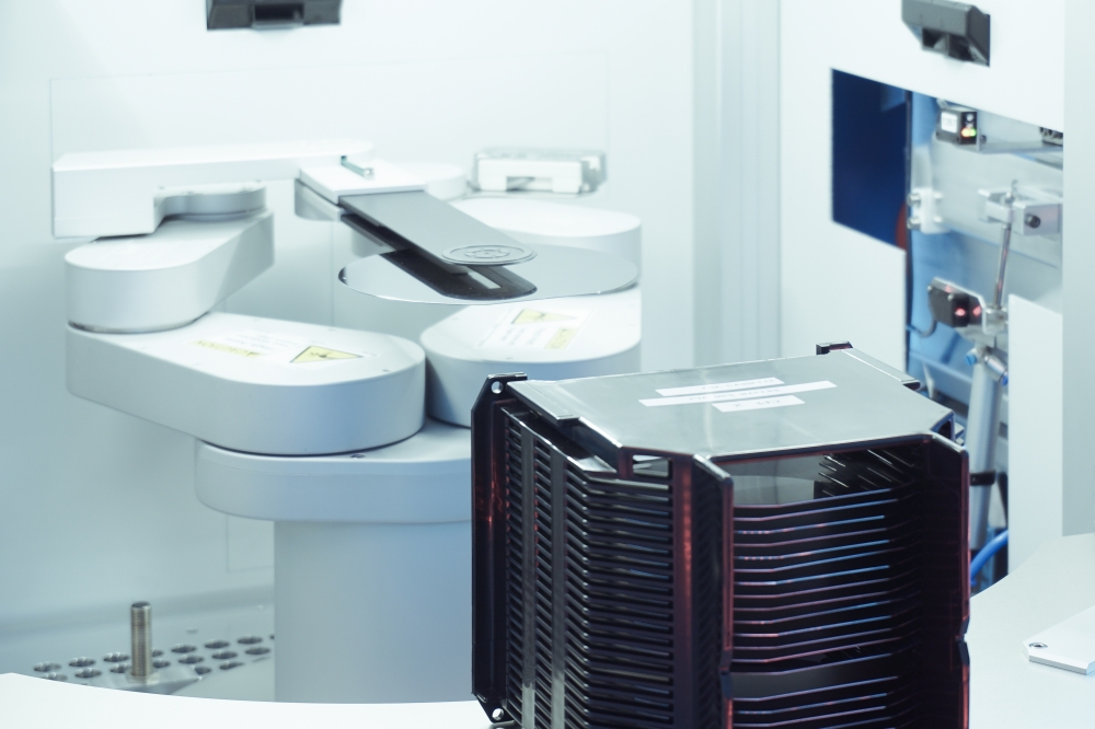
In manually loaded systems, the asher has a pull-out door where the wafers lie on the heating or cooling plane mounted on the entry door of the chamber. In automated systems, wafers are increasingly loaded into the chamber utilizing robotic handling.
“Today, customers want to reduce all human factors as chips continue to become more advanced,” said Pleyer. “This requires automatic handling and loading using robotics and full control by a host computer. In some cases, the operator only needs to place the cassette onto the load port, which will start automatically.”
PVA TePla, for example, has designed its GIGAfab-A plasma system to be configurable for 200- or 300-mm wafers and a cluster tool with up to 3 process modules called the GIGAfab Modular. Both systems use open cassette as well as front opening or standard mechanical load stations. Wafer processing is thermoelectrically controlled from RT to 250°C. A unique planar microwave plasma source provides high ash rates over a wide temperature range.
With wafers becoming thinner, more reliable automated single wafer processing equipment handles fragile wafers.
“Trying to handle the wafers physically without the use of robots can end poorly,” says Ryan Blaik, sales manager of semiconductor and medical devices at PVA TePla in California, Single wafer processing also provides better temperature controls.
“With batch processing, microwave radiation must heat all the wafers in a quartz boat, and the temperature can fluctuate during processing,” says Blaik. “For a single-wafer processing system, wafers are brought into the chamber only after pre-heating, allowing a constant temperature to be maintained during processing.”
In single wafer processing, a descum process can be accomplished using the same tool. The primary difference between the two processes is the temperature the wafer is exposed to while in the plasma chamber.
According to PVA TePla’s Pleyer, “For descum, we want a low ash rate and good uniformity and process control. Because we are only targeting removal of residues, an ashing recipe at very high temperatures will not work. It is easier to accomplish using single wafer ashing using a microwave-based plasma system.”
As more semiconductor device fabrication continues to ramp up globally to meet an insatiable demand for chips, the need for control, efficiency, and configurable solutions for wafer ashing will continue as the chips themselves increase in complexity and decrease in size. Automated, single-wafer microwave plasma systems provide chip fabricators with targeted and configurable ashing that meets the needs of an increasing array of wafer types.


