Breaking new ground with the hybrid transistor
A unique integrated manufacturing process creates hybrid transistors
that unite the low on-resistance of GaN HEMTs with the non-destructive
breakdown of SiC diodes
BY AKIRA NAKJIMA FROM THE NATIONAL INSTITUTE OF ADVANCED INDUSTRIAL SCIENCE AND TECHNOLOGY
Our planets's temperature is on track to rise to levels that will have horrendous consequences for humanity. Due to this, it is critical that global carbon emissions fall fast. To succeed, we must act on many fronts, including adopting new approaches to the way that energy is created, distributed and used.
If we are to move to a greener society, we will need to change the way we produce and use most of our electricity. Such efforts will have to consider the electrical power converters that step up and down the voltage and transfer it from DC to AC or vice-versa – these are the ‘power bricks’, extensively employed in a number of electronic applications, including the power supplies in PCs, telecommunications, electric vehicles and aerospace applications. Trim the power losses in these converters and boost their efficiency, and this will lead to energy savings at the system level.
Shifting to a low-carbon society will also require an increase in the uptake of electric vehicles, alongside the installation of far more wind turbines and solar farms. For all these green technologies, we need power converters that are smaller, more efficient and more reliable than the incumbents. To realise this, there will have to be further technological innovation in the power transistors used in the converters.
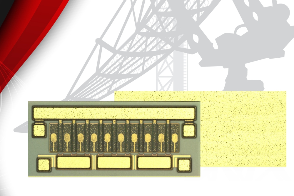
Figure 1. Photograph of fabricated hybrid HEMTs on a 100 mm SiC substrate (left) and an equivalent circuit (right).
At the heart of power-conversion circuits are power transistors, performing the role of a switch. Ideally, these devices should combine a low on-resistance, to ensure a low conduction loss in the on-state, with a fast switching performance that trims switching losses.
Silicon power transistors are widely deployed in converter applications. Thanks to extensive research and development since the 1960s, their performance has improved, but now it is encroaching material limits. Thus, to deliver higher efficiencies, there’s a need to turn to a different class of semiconductor. This has led to much interest in devices formed from semiconductors with a wider bandgap. One of them already enjoying commercial success is the GaN HEMT, which features a high-density, highly mobile two-dimensional electron gas (2DEG) as a channel, generated by the unique polarisation nature of the AlGaN/GaN heterointerface (see Figure 2(a)).
Figure 2. (a) Schematic cross-section of a conventional GaN HEMT and a (b) silicon DMOSFET.
The mobility in this channel can exceed 1500 cm2 V-1 s-1, due to the generation of free electrons without impurity doping. Another strength of this transistor, resulting from the high electric field strength of the material, is that control of the 2DEG can be realised at a concentration as high as 1013 cm-2 – that’s one order of magnitude higher than that for GaAs and silicon devices. Armed with these attributes, the GaN HEMT surpasses the silicon limit, in terms of low resistance and fast switching.
It is now many years since researchers reported the first GaN HEMTs in the 1990s. Subsequent development and commercialisation has led to their deployment in power converters of less than approximately 3 kW, such as compact AC adapters for smartphones, where they combine high efficiency with miniaturisation.
Unfortunately, GaN HEMTs suffer from reliability-related issues, hampering their deployment in high-power applications, such as electric vehicles. An impaired robustness arises from a behaviour that differs from the incumbent, the silicon double-diffusion MOSFET (see Figure 2 (b)). In this double diffusion MOSFET, there is a p-n junction between the p-type base region and n-type drift layer, as well as a p-n diode – known as the ‘body diode’ – that is connected in an anti-parallel configuration (the equivalent circuit is shown in Figure 3(a)). With this configuration, applying an overvoltage to the DMOSFETs under abnormal circuit operations causes the body diode to undergo a non-destructive avalanche breakdown, with the noise energy absorbed as Joule heat in the silicon chip. Due to this, when silicon power transistors are used in converter circuit topologies, they tend to prevent overvoltage during abnormal operations, thereby ensuring system reliability.
Figure 3. Equivalent circuits in (a) silicon DMOSFETs, (b) GaN HEMTs and (c) hybrid HEMTs in this study.
With GaN HEMTs, it’s a very different state of affairs. The GaN HEMT does not have a body diode, so there is no pass for the noise energy to escape, causing this form of transistor to be destroyed by overvoltage. This weakness has limited the energy saving provided by the GaN HEMT to just low-power converters.
Figure 4. Schematic of off-state breakdown characteristics in silicon DMOSFETs and GaN HEMTs.
Uniting GaN and SiC
At the National Institute of Advanced Industrial Science and Technology our team has developed an approach to addressing this weakness, based on the introduction of a hybrid HEMT that combines GaN and SiC. This novel transistor, which solves the issue of destructive breakdown, features a SiC-based anti-parallel p-n diode, monolithically integrated to a GaN HEMT (see Figure 5(a)) for a diagram of this device, and Figure 3(c) for the equivalent circuit). This hybrid device has five electrodes: the source, gate and drain of the GaN HEMT structure; and the anode and cathode of the SiC diode structure.
Figure 5. (a) Schematic of a GaN/SiC-based hybrid HEMT. Five electrodes:
source (S), gate (G), and drain (D) in the HEMT; and anode (A) and
cathode (C) in SiC diode. (b) Our fabrication process flow for GaN/SiC
hybrid HEMTs.
Operated in its off-state, this hybrid can undergo non-destructive avalanche breakdown in the SiC body diode, ensuring robustness. Turn this device on and current flows through a 2DEG channel at the AlGaN/GaN interface, enabling a low on-resistance. So, thanks to these modes of operation, our hybrid HEMT combines the merits that really matter.
To produce our novel devices, we expanded a 100 mm SiC-based prototyping line, located at an open innovation facility in Tsukuba, Japan. Our changes created a prototyping line for fabricating SiC, GaN and hybrid devices. With these modifications, we have been able to fabricate hybrid HEMTs that are small in size and have a gate width of 50 µm.
The steps we take to make our devices (summarised in Figure 5(b)) begin with the growth of p-type SiC via CVD. After this, we form p-type and n-type SiC regions by ion implantation and activation, before growing HEMT layers by MOCVD and defining the mesa structures by dry etching. Electrodes are then added, followed by deposition of a 3 µm-thick aluminium layer that provides the pad metal. Our final steps involve covering the surface with a polyimide and depositing a nickel-based alloy on the backside of the device.
Electrical measurements on our hybrid HEMT produce promising results. Unlike typical GaN HEMTs, they are not destroyed immediately after a breakdown, but undergo a non-destructive avalanche breakdown in the SiC diode – this is accomplished by designing the breakdown voltage of the SiC side to be slightly lower than that of the GaN side. The breakdown behaviour, associated with a breakdown voltage of about 1.2 kV, is shown in Figure 6(a). As the avalanche breakdown is non-destructive, our device offers a stable reversible breakdown during multiple sweeps. Operating under forward bias, our hybrid HEMT produces a drain current as high as 300 mA/mm and an on-resistance of just 47 Ω mm, thanks to current flow through a high-mobility 2DEG (see Figure 6(b)).
In addition to the low on-resistance and the non-destructive breakdown, our hybrid transistor offers excellent heat-dissipation characteristics. This particular attribute comes from the excellent thermal conductivity of SiC, which is three times that of silicon.
Figure 6. (a) Measured off-state breakdown of the fabricated hybrid
HEMT. Repetitive current-voltage (I-V) sweep curves up to 2 mA/mm show
high stability against avalanche current stress. (b) On-state
characteristics. Owing to current flow via the low-resistance 2DEG, a
low on-resistance of 47 Ω-mm and high saturation current of 300 mA/mm
were measured.
Other marriages
Our hybrid HEMT has great potential, combining excellent traits under forward and reverse bias with excellent thermal management. These are very encouraging signs for a device that is still in its infancy, with much opportunity lying ahead for optimisation of the device structure and its fabrication process. Our next steps will be directed at demonstrating large-area devices, rated at 10 A or more, that can be used in actual power converters. We will also devote much effort to trying to commercialise this technology, by engaging with companies that have technical expertise in power devices.
Our work forms part of a global effort at developing power devices from materials with a much wider bandgap than silicon. SiC and GaN devices are now commercialised, while those with an even larger bandgap, such as the promising trio of Ga2O3, AlN and diamond, are attracting much attention. Of those three, diamond has the potential to be the ultimate semiconductor, due to its extremely high field strength and its superior thermal conductivity.
However, heterogeneous integration of different semiconductors may offer new, unconventional opportunities.
Our hybrid HEMT highlights how integration can deliver performances not possible with a single material. There are numerous combinations to explore, opening the door to novel device concepts. We are aiming to investigate what may be possible with this approach, and how it could unleash a new generation of power devices.


