Branching out to gallium oxide
Bristol University academic Martin Kuball is expanding his areas of
expertise from the analysis of wide bandgap devices to the growth and
production of gallium oxide transistors.
INTERVIEW BY RICHARD STEVENSON, EDITOR, COMPOUND SEMICONDUCTOR
RS: What excites you about gallium oxide, compared with the more common compounds for making power devices, silicon carbide and gallium nitride?
MK: Gallium oxide has a greater bandgap and can be made quite cheaply. Researchers have already produced 4-inch to 6-inch gallium oxide substrates and grown on them. This opens a huge opportunity for this ultrawide band gap material to enable high-performance, low-cost power electronics. Devices could operate even in excess of 10-12 kilovolts; or maybe compete against silicon carbide in the 1-2 kilovolt range, with a little less performance, but greatly cheaper.
Maybe gallium oxide will also get more young people into semiconductors. This is an exciting field for careers. I was at a conference last week, and a lot of people asked me: Do you have people who could work for us in our semiconductor company?
RS: Over many years, you and your team have provided great insight into the thermal management of wide bandgap devices, using techniques such as micro-Raman spectroscopy. These investigations have involved analysing devices provided by other groups. Rather than continuing this approach with gallium oxide, you’ve installed an MOCVD tool so you can make your own devices. What prompted you to move into growth when branching out into gallium oxide?
MK: When I came from Brown University to Bristol University in 1997 I started with optical spectroscopy. From this I built very strong expertise in the thermal management of devices. I worked at that time with QinetiQ, with TriQuint, which is now Qorvo, and with many other suppliers. We developed ways to measure the thermal characteristics of devices, such as the device temperature with a very high spatial resolution. From there we expanded into other techniques, such as how to measure the thermal conductivity of materials, and we spun out TherMap Solutions. For our next step, we built strong expertise in electrical characterization, device reliability and the design of devices.
Since it’s at a very early level of development, gallium oxide device and material availability is limited. We have great collaborations with people in the US, in Japan and in Germany, but having growth directly here opens huge opportunities to fully benefit from our device expertise. We can grow the material structures we want with specific dopants, fabricate devices and analyse them. We can understand from the growth side what we need for the device side and vice versa, so we have this great interlinking of knowledge.
We will continue working with the people in the US, Germany, Japan, and other places who we worked with before. But we will also make new links, when we grow material and when we make devices. We’re more than happy collaborating with people, because we want to help accelerate gallium oxide.
RS: What facilities do you have for processing epitaxial materials into devices?
MK: We have a sizeable cleanroom. It’s in the same building, on the level underneath the MOCVD system. The cleanroom has all the necessary tools for photolithography. We have e-beam lithography, we have etching tools, and we have ALD for depositing oxides, and so on, so we do full device processing at Bristol University.
RS: Gallium oxide can be grown by a variety of techniques, such as MBE, HVPE and mist-epitaxy. Why are you pursuing MOCVD?
MK: To take full advantage of gallium oxide’s properties, you need vertical devices, to push the breakdown voltages as high as you can. MBE is a very slow growth technique. We have lateral devices made by MBE, but our main focus is actually on vertical devices.
HVPE is the optimum technique to make very thick layers. It is a very fast growth technique, but you tend to have more impurities, at least in the nitrides – the oxides probably still need to be looked at.
With MOCVD, we have very good control of impurities and the possibility to make very sharp interfaces. We’re going to look at heterogenous integration of gallium oxide with other materials. This was a reason for doing MOCVD.
RS: What considerations must be made when deciding to install an MOCVD reactor for gallium oxide growth?
MK: Installation is quite easy to do. You don’t need expensive scrubbers, as you would have on a gallium nitride system, for example, as the output is not that toxic.
To grow clean materials, you need to have very clean gas lines. Our installation involved a great team of local engineers and hired external contractors. Our pipework is designed to fulfil the highest specifications we need for growing very high-quality layers of gallium oxide and aluminium gallium oxide.
RS: Did you consider building your own reactor?
MK: We could have spent a few years building our own system, but I’m more interested in getting to the device side. It is much better for us to work with people who have spent a lot of time designing a good gallium oxide growth system. We worked with Agnitron. They have done a lot of prior research and investment, and have a very good track record in commercial gallium oxide MOCVD systems.
RS: How easy is it to source substrates for the epitaxy of gallium oxide?
MK: It’s quite easy. We buy from a commercial supplier, NCT in Japan, and work with other suppliers. There’s an emerging activity from Northrup Synoptics, and there are other upcoming suppliers.
RS: What’s going to be the first type of device you make?
MK: The first devices will be lateral devices. They will be test structures, to understand the growth, to understand the interfaces, to understand trap densities and see what breakdown voltages we can get. The second type of device will be trench Schottky barrier diodes and FET devices, vertical devices.
We will first reproduce what other people have done, just seeing where we stand compared to published data.
The third generation will be the integration of gallium oxide with other materials to engineer some issues out, such as the low thermal conductivity of gallium oxide and its lack of workable p-doping.
This is a current plan. I’m pretty certain we will revise this plan as we go along to maximise the device performance, including reliability.
The ultimate goal would be a 10-12 kilovolt device. We will start aiming at 1, 2, 3 kilovolt devices and work ourselves upwards. We’ll also make comparison against silicon carbide technology.
There’s so little known about the reliability of gallium oxide devices, so we will definitely look at that side, with our track record in device reliability. We will look at how you optimise surfaces and how you optimise materials to minimise trap states. We will find ways to make optimal heat sinking.
The roadmap will say ‘let’s aim for a 12-kilovolt device’, but there will be many, many steps in between.
RS: You’re also doing some growth on sapphire, aren’t you?
MK: Yes. Sapphire is naturally easy to source. This is a low-cost substrate.
We also have the intention to grow on other substrates. Recently, from the simulation perspective, we showed the benefits of integrating n-type gallium oxide with p-type diamond. There’s a lot of other substrate materials we will look at in this context. Gallium oxide has a low thermal conductivity, it cannot easily be doped p-type; but even if you can dope it p-type, the valence bands are very flat, so you get hole trapping.
We’ve done a lot of gallium-nitride-on-diamond integration. That was mainly for RF devices; these will always generate a lot of heat. 20, 30, 40 percent of the power is going to be exiting as heat. But we’re looking here mainly at power devices. A good power device mainly generates heat at the point when you switch the device. So, in the optimal case, in the off-state there is no current flow; and in the on-state, the resistance is very small. So you won’t actually have a lot of heat generation. When you switch it, you will have a voltage and current flow, so during the switching state you generate heat. The heat generation is much less than in an RF device and thermal management is less critical. But if you really push the Ampere rating of the device, you have to worry about that.
RS: You’re planning to make some heterostructures that combine gallium oxide with aluminium gallium oxide. Where might that lead?
MK: There’s very beautiful work by a group in Ohio, who looked at heterostructures and showed that you can get nice mobilities at interfaces. We will look into this. There’s also work on multi-channel devices, and we will look at aspects of this.
There’s also just the point of curiosity: how can you change material properties, if you do superlattices? How can you increase the potential of gallium oxide?
RS: Is it easy to apply the techniques you developed to look at the thermal management of devices made from gallium nitride and silicon carbide to those made from gallium oxide?
MK: Historically, we developed a lot of device and materials characterization techniques. Many of them focused on gallium nitride. All are applicable to gallium oxide, and we will use them – the thermal management characterization, Raman thermography; and transient thermoreflectance.
We recently developed a technique to map electric fields in gallium nitride devices, based on second-harmonic generation. We published an account of this in Nature Electronics, and we have an additional paper just accepted in Applied Physics Letters. A few smaller things will need to be modified in the setup for gallium oxide, but it’s an exciting opportunity to, for example, optimise edge termination in gallium oxide devices.
The whole electrical characterization suite we have developed will naturally also apply to gallium oxide, from DLTS-style methods to look at trap states to dynamic R-on, pulse and double pulse IVs, as well as reliability assessments. They are easy to apply. It doesn’t need much change.
RS: As well as leading a large and expanding research group, you’ve taken a very active role in conferences. In 2019 you organised Diamond D Day, a one-day conference attracting 120 delegates, half from overseas. You have just come back to CS Mantech, where you held the role of technical programme chair. Obviously, in your mind, conferences are an important part of driving research?
MK: Conferences are an important part of bringing people together to discuss and move research forward, first presenting the latest data and then discussing it, brainstorming ways forward and getting new ideas.
A few years ago we ran Diamond D Day in Bristol. Covid has prevented us running this again. But I’m certain in a year or two we may run a Diamond D Day Two, on the integration of diamond with gallium nitride and other semiconductors, such as gallium oxide.
In different roles, I’ve been involved in CS Mantech for probably the last ten years. I was technical programme chair of the conference this year in Monterey, California. This conference brings a lot of industry together. From the attendees, it’s probably 70, 80 percent from industry; and 20 percent students, faculty. It’s very interactive, very positive, with lots of brainstorming, and this is extremely important.
Next year CS Mantech will be in Orlando. I will be overall chair, and I will push for more ultra-wide bandgap materials and devices in this conference. This year, I believe we had two, three or four talks on gallium oxide at CS Mantech.
RS: Do you think that conferences that cover compound semiconductor technologies are well suited to helping those in academia and industry interact? Or are there are some barriers that need to be broken down?
MK: There can be barriers. Some industries may be reluctant to work with academia for different reasons, for example, IP. Academia may be sceptical working with industry because the project may be too short term. Collaborations must find a sweet spot of interactions.
I have worked with industry probably since the day I started in Bristol, 25 years ago. Conferences are a useful tool to initiate that. CS Mantech has been very good in my own personal career, establishing links with industry. Some of my current industrial interactions go back to discussions I have had with companies at CS Mantech. This year I had very useful conversations with three, four, maybe five companies; this hopefully leads to interaction.
You’ll find a good array of conferences. Some have a larger industry participation, like CS Mantech; and some, like IWN and ICNS, have less industry interaction. You need that balance, where in some cases you do blue sky research and maybe don’t interact with industry. But still industry can listen to that. Maybe that doesn’t lead to interaction – that’s fine.
RS: One of the motivations for developing and producing wide bandgap power electronics is to save energy and try and reduce carbon footprints, while many international conferences involve a lot of flying. Do you see that as a conflict? And what do you think lockdowns associated with Covid have taught us about pros and cons of online gatherings?
MK: It’s always a challenge to go to a conference developing carbon-emission-reducing technologies and having to fly. Conferences are important for face-to-face discussions. They can’t replace Zoom or Teams meetings. On the other hand, not everything has to be done flying around the planet.
Covid had a lot of negative impact on people, personally, and on business and the economy. We’re hopefully slowly moving to a point past Covid, where we can naturally return to conferences where people are present, such as CS Mantech this year. But equally, we must take advantage of all the online tools developed during the last two years. When Covid started, they were not as good as they are now. They have improved a lot.
Yesterday I had a meeting with people in the US. This brought six-to-seven people together for an online meeting. It was a perfect information exchange, brainstorming how we can collaborate together. I didn’t need to do this as face-to-face, flying over.
Having a combination of conferences, but also taking advantage of the online tools, will hopefully reduce the amount of flights and travel people do, but equally provide an even better outcome. With this approach, I can actually talk to more people. I can talk to someone in Japan in the morning, and someone in the US in the afternoon. We should take this as the positive side from the Covid evolution, making use of the online tools developed.
During 25 years at Bristol University, Martin Kuball (far right) has built up a team focusing on wide bandgap technologies that now numbers around 20 researchers. Key members of the team involved in gallium oxide growth are post-doctoral research fellow Indraneel Sanyal (centre) and PhD student Arpit Nandi (left).
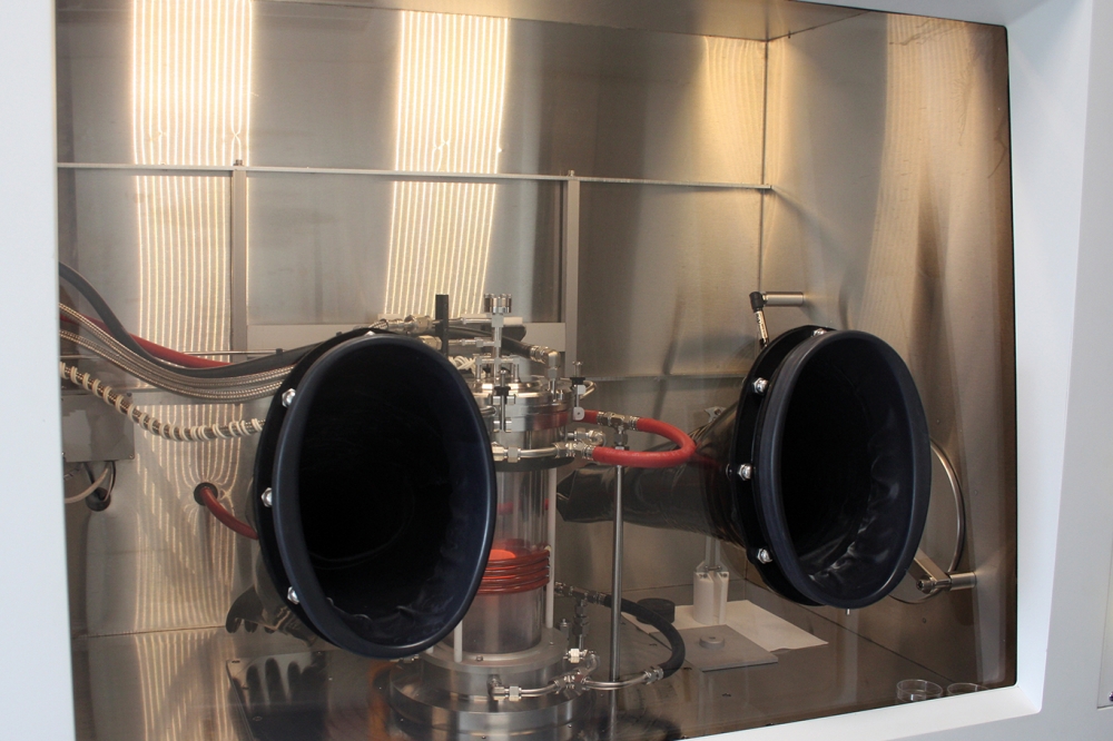
Earlier this year, Martin Kuball’s group at the University of Bristol, UK, installed an Agnitron MOCVD reactor for the growth of gallium oxide and related materials.


