

Progressing the photonic-crystal surface-emitting lasers
Thanks to a number of advances, photonic-crystal surface-emitting lasers
(PCSELs) now combine a high output power with great beam quality,
polarization, beam-pattern control and on-chip two-dimensional beam
scanning.
BY SUSUMU NODA FROM KYOTO UNIVERSITY
Semiconductor lasers continue to make important contributions to our society. They are deployed for many tasks and have made significant and lasting contributions to communication networks and optical storage. In these settings, much effort has been devoted to expanding the utility of this source by widening its range of emission wavelengths and increasing its modulation speed.
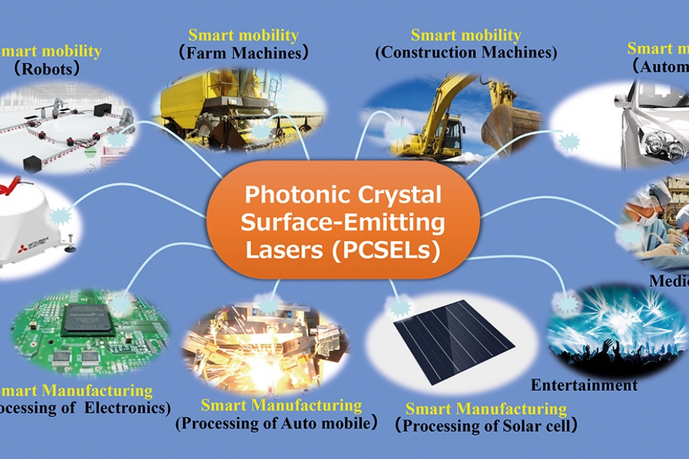
There are also opportunities for lasers in Smart Mobility and Smart Manufacturing. However, conventional lasers that are designed for these tasks produce a very broad spectral emission and struggle to meet the high output powers and high beam qualities that are required (see Figure 1 left ).

Figure 1. Comparison of conventional broad-area semiconductor laser and a PCSEL.
Like many other classes of laser, those made from semiconductors have additional areas for improvement. Today’s chips are incapable of providing an on-chip beam pattern, polarization and direction control. Failing to offer these functionalities is a significant weakness – these omissions have to be addressed with external elements, and this forfeits the advantage of compactness, for which semiconductor lasers are renowned.
Fortunately, this paradigm can change, thanks to the development of the PCSEL, an acronym for the photonic-crystal surface-emitting laser (see Figure 1 right). This device is currently attracting much attention, because it can realise simultaneously a high output power and a high beam quality, and offer functionalities that are not easily achievable with other types of laser, such as polarization and beam-pattern control, as well as on-chip beam-direction control, which eliminates the need for bulky external optics.
The remainder of this feature offers a brief overview of the history of the PCSEL, along with an account of recent progress, including success associated with newly developed photonic crystals.

Figure 2. Progress of PCSELs.
The PCSEL’s past
Our team from Kyoto University proposed and demonstrated the concept of the PCSEL back in 1999. The key characteristics of this class of laser are its operation at a singularity point ⌈(of two-dimensional (2D) photonic crystal, which has a lattice formed from two types of materials with a large refractive index contrast, such as air and a semiconductor. In this high-contrast lattice – it could be square, triangular, or of another form – there is coupling of fundamental (first-order) Bloch waves and higher-order Bloch waves. Due to this interaction, the PCSEL is capable of a broad-area 2D coherent lasing oscillation. The nature of the ⌈point ensures that emission comes from the surface of the photonic crystal; it is for this very reason that we named this laser the PCSEL.
It is worth noting that the PCSEL is different from the 2D distributed feedback laser. As the latter has a smaller refractive index contrast, due to alternating layers of differing semiconductor materials, coupling is only between fundamental waves. Due to this limitation, there is no coherent 2D resonance of the transverse-electric modes in square-lattice structures. For this reason, it is difficult for an ‘all-semiconductor’ PCSEL to realise coherent operation over a 2D broad area.
Following our initial demonstration of the PCSEL at the end of the last century, we have kicked on to develop its basic operating principles and a number of new functionalities. We reported our realisation of polarization mode control in 2001; the development of beam pattern control in 2006; our introduction of blue-violet wavelength emission, using GaN materials, in 2008; one-dimensional beam steering in 2010; and watt-class operation with a high beam quality in 2014. As well as the triumphs in the lab, a 0.2 W class device that’s based on these photonic crystals has been commercially available since 2013 (see Figure 2 for a timeline of success).
In addition to all this success, recently we have enjoyed further breakthroughs, which have come from optimising the photonic crystal structure. In 2018-2019, we unveiled a unique photonic crystal structure that we call a ‘double-lattice photonic crystal’. This architecture ensures a high beam quality and can realise a PCSEL output power of 10 W or more. We have also introduced, in 2020, a ‘dually modulated photonic crystal’ PCSEL. Its hallmark is to provide two-dimensional control of beam diffraction while simultaneously preserving two-dimensional resonance.
Boosting brightness
The merits of high power and high-beam-quality associated with the PCSEL come together to ensure high brightness. This characteristic is defined as the optical power, per unit area, per unit solid angle; this metric provides a figure-of-merit for how intensely a laser beam can be focused, and how narrowly an emitted laser beam diverges.
Brightness is proportional to the size of the device, and inversely proportional to the product of lateral modes in orthogonal directions. In conventional broad-area semiconductor lasers, the well-trodden path to realising a higher output power is to increase the size of the device, but this comes at the expense of an increase in the number of lateral modes. Consequently, this approach fails to boost brightness. It’s a similar story with the VCSEL, but not with the PCSEL, because with this particular laser it is possible to have very few lateral modes – ideally, they can be single – while increasing the size of this device (see Figure 1 right, again). Thanks to this asset, PCSELs are expected to operate with a brightness of 1-10 GW cm-2 sr-1, a level of performance associated with large lasers, such as CO2 lasers and fibre lasers. What’s more, PCSELs have the potential to produce a lasing spectrum that is very narrow, and ideally single mode, as well as a temperature dependence that is far smaller than that of conventional, broad-area semiconductor lasers.
To increase the brightness of our PCSEL, we have introduced a double-lattice photonic crystal. This consists of two square lattices with larger and smaller lattice points, whose positions are shifted by around one-quarter of the lattice constant. This design ensures that light waves are diffracted by individual lattices with an optical-path difference of half-a-wavelength. Due to this, destructive interference occurs for 180 ° diffraction, leading to a spreading of the light field (see Figure 3). As the antinode of the higher-order mode is close to the edge of the device, the higher-order mode is cut off, leading to a high beam quality and ultimately a high brightness.

Figure 3. Impact of double-lattice photonic crystals.
We have fabricated a PCSEL with a double-lattice photonic crystal, mounting this chip on a package in an up-side down configuration, with the output beam emitted from the substrate side (see Figure 4, left). Measurements reveal that when operating in pulsed mode, this source produces an optical output of more than 20 W at a slope efficiency of 0.83 W/A. Thanks to a very narrow beam divergence of 0.1 °, brightness exceeds 1.5 GW cm-2 sr-1. As well as these great characteristics, our PCSEL with the double-lattice operates stably in a single mode from -40°C to 100°C, and has a temperature dependence of just 0.08 nm/°C. If a higher slope efficiency is needed, PCSELs can be combined in series. By configuring a three-element array in this manner, we have increased the slope efficiency to more than 2.3 W/A.

Figure 4. (Left) PCSEL mounted on 5.6 mm-diameter package, (middle)
I-L characteristic (inset shows the far-field pattern (FFP)), and
(right) temperature dependence of lasing spectra.
One of the emerging opportunities for high-brightness PCSELs is in lidar, a technology needed for Smart Mobility of cars and robots (see Figure 5). To highlight the capability of a PCSEL for these applications we have provided a proof-of-concept demonstration, where this source lies at the heart of a compact, simplified time-of-flight lidar system.

Figure 5. A typical lidar system (time-of-flight (ToF) type).
Our evaluation of this system began by considering how small its beam diameter can be maintained when the emitted beam propagates in free space without the assistance of any external lens system. We projected the beam on a screen placed at distances varying from 15 cm to 30 m, and compared our findings with those for a conventional broad-area laser (see Figure 6).

Figure 6. Comparison of a far-field beam propagation of a conventional semiconductor laser and a PCSEL.
As one would expect, the beam from the conventional broad-area laser spreads out quickly, because its divergence angles are large and asymmetric. Due to this limitation, we could not discern the beam’s pattern after it had travelled beyond 1 m. In lidar systems this weakness is addressed by employing an external, complicated lens arrangement alongside conventional lasers. However, this solution adds complexity and increases the size of this unit.
It’s a markedly different situation with a PCSEL-based lidar. Thanks to far smaller divergence angles, the beam diameter is far smaller, even at distances far from the laser. Remarkably, even at 30 m, the diameter of the circular beam is below 5 cm, in terms of its full-width at half-maximum. This promising result indicates that when a PCSEL is used in a lidar system, it does not require an external lens system and its associated complicated adjustment process. This can cut the cost, weight and size of a lidar system.

Figure 7. Comparison of a conventional semiconductor laser and PCSEL light sources for lidar.
Encouraged by our findings, we have gone on to develop lidar systems that incorporate our PCSELs (see Figure 7 for a comparison with a lidar system featuring a conventional laser). In these systems, laser beams are scanned in one dimension by mechanically rotating a mirror. Attempting this with a lidar featuring a conventional laser is hampered by a large, distorted beam spot, even after a complicated system of lenses is employed to reshape the beam. Due to distortions in that system, beam spots overlap during beam scanning, lowering the system’s spatial resolution. In sharp contrast, our PCSEL-based lidar provides clearly separated beam spots during beam scanning, and ultimately a high spatial resolution.

Figure 8. Demonstration of lidar with a PCSEL light source.
Using a PCSEL-based lidar system that we built in 2020, we have undertaken distance measurements in real time (see Figure 8). This system captures fine details of the motion of Persons A and B, such as the movement of their hands, illustrating the superiority of a PCSEL-based light source. In 2021 we built on this success, slashing the volume of a PCSEL-based lidar by a factor of three (see Figure 9).

Figure 9. Further miniaturization of a lidar system. The 2021
version is just one-third of the volume of its predecessor from 2020.
High-brightness PCSELs are not limited to pulsed operation. We have also produced continuous-wave variants, increasing the diameter from 500 µm to 1 mm to aid heat dissipation. For this device, with a design optimised for its diameter, a 10 W CW output is possible while retaining a very narrow beam divergence angle.
We have applied this high-brightness CW PCSEL to the marking of a metal surface. If you look at Figure 10, you can see “PCSEL” written clearly.
Very recent progress by our team has led to the fabrication of a PCSEL that produces a 30 W output, realised by scaling the diameter of this emitter to 2 mm. This success offers a roadmap to 100 W and even 1 kW CW operation, by expanding the size of the PCSEL to 3 mm to 10 mm. Realising such higher powers would allow the PCSEL to replace very large lasers, such as CO2 lasers and fibre lasers, and become the key light sources for Smart Manufacturing.
Armed with attributes
When used for lidar, one of the advantages of the PCSEL over the conventional laser is its superior beam quality that allows the use of a mechanically rotating mirror. But if rather than using a mechanical means for scanning, this could be accomplished with an electrical approach, the system would take a leap forward in terms of reliability, stability, and compactness.

Figure 10. (Left) CW operation of PCSEL with a size of 1mm in diameter.
(Right) Marking experiment onto metal (stainless) surface.
Motivated by the potential to deliver a dramatic improvement in system performance, we have recently developed a PCSEL that is capable of electrical beam scanning in two dimensions. This triumph has built on our electrical beam scanning in one dimension, reported in 2010. To progress from scanning in one direction to two, we have advanced our photonic crystal structure. By creating what we describe as a dually modulated photonic crystal, we have been able to produce a laser that emits a high-power, high-quality beam in an arbitrary direction in two dimensions.
To produce a PCSEL that has electronic beam scanning in two dimensions, we simultaneously modulate the positions and sizes of the lattice points of the photonic crystal (see Figure 11). A crucial difference between the design of this particular PCSEL and its forefathers is that it has a different singularity, known as the M point, adopted to inhibit the emission of light prior to modulation. Introducing dual modulation to this design ensures that the beam is only emitted in the direction of one’s choosing.

Figure 11. Scanning-electron-microscope image of a dually modulated
photonic crystal (bird’s-eye view). Lattice-point positions and sizes
are simultaneously modulated. These modulations encode information about
the beam emission direction. Also, the lattice constant (equal to the
spacing between the lattice points) is set to 1⁄√2 times the wavelength
in the material ( 195 nm).
We have fabricated an on-chip 10 by 10 array of dually modulated PCSELs: each individual laser has a footprint of 150 µm2 and a circular current injection area with a 100-µm diameter. All electrodes are integrated onto the back of the chip, so that the laser beams are emitted from the front without obstruction (see Figure 12). To address the array, PCSELs are electrically isolated from each other, and only the PCSEL(s) at the intersections of p- and n-line electrodes across which a voltage is applied are driven. Each PCSEL is encoded with its own unique beam emission direction. From each PCSEL two beams are simultaneously emitted at oblique angles, which are mutual reflections of each other about the surface normal.

Figure 12. On-chip array of dually modulated PCSELs for beam emission in
various directions in two dimensions. (Top) schematic of the entire
device. (Bottom) microscope image of the bottom of the chip.
With our arrayed chip we can drive 100 PCSELs in any order, and at any speed. This capability, illustrated in Figure 13, offers just one example of beam scanning; in general, various beams can be scanned in any order, at any timing. It’s also worth noting that the number of resolvable points is not limited to 100 – in fact, it can be increased to over 90,000 without considerably increasing the chip area. Furthermore, it is possible to construct a new type of lidar system that leverages this beam-scanning technology; the combination of flash- and beam-scanning lidars, a topic we are planning to discuss elsewhere.
This latest success is yet another example of our efforts to strengthen the research and development of the PCSEL and drive its deployment. To support this endeavour, we have recently established the Center of Excellence for this device. We are keen to share what we have realised, and can provide PCSEL samples for testing, provided under a material transfer agreement.

Figure 13. Example of multi-beam scanning using a lasing wavelength of
940 nm. The top row of snapshots show beam scanning when the n-line
electrodes are driven in sequence from n-1 to n-10 while the p-line
electrode is fixed to p-5. For this sequence, a fixed polar emission
angle θ (from the surface normal) of 20 ° has been encoded, while
azimuthal emission angles θ (from the positive x axis) have been encoded
to vary from 0 °/180 ° to 45 °/225 °; these emission angles are
precisely those observed in the snapshots. Next, the middle row of
snapshots shows beam scanning when the same sequence of n-line
electrodes is driven, but the p-line electrode is fixed to p-6. In this
case, it is the azimuthal angles θthat have been designed to remain
fixed to 90 °/270 °, while the polar angle θ has been designed to vary
from 0 ° to 45 °; again, these emission angles are precisely those
observed in the snapshots. Finally, the bottom row of snapshots shows
beam scanning when the electrodes in the top and middle rows are driven
at the same time to scan four beams simultaneously.
This work constitutes a portion of the research performed by Noda’s Quantum Optoelectronics Laboratory in conjunction with the Nano processing Lab at Kyoto University. The authors are deeply grateful to faculty members, researchers, and students of both laboratories. This work was carried out under the project of Council for Science, Technology, and Innovation, Cross-minesterial Strategic Innovation Promotion Program, Photonics and Quantum Technology for Society 5.0 (Funding agency: QST), and under the CREST program Next-generation Photonics commissioned by the Japan Science and Technology Agency .
Further reading
† https://pcsel-coe.Kuee.Kyoto-u.Ac.Jp/
† M. Imada et. al. Appl. Phys. Lett. 75 316 (1999)
† S. Noda et. al.. IEEE J. Sel. Top. Quantum electron. 23 4900107 (2017)
† M. Imada et. al. Phys. Rev. B 65 195306 (2002)
† S. Noda et. al. Science 293 1123 (2001)
† E. Miyai et. al. Nature 441 946 (2006)
† H. Matsubara et. al. Science 319 445 (2008)
† Y. Kurosaka et. al. Nat. Photonics 4 447 (2010)
† K. Hirose et. al. Nat. Photonics 8 406 (2014)
† https://www.Kyoto-u.Ac.Jp/static/ja/news_data/h/h1/news6/2013/130926_1.htm
† M. Yoshida et. al. Nat. Mater. 18 121 (2019)
† R. Sakata et. al. Nat. Commun. 11 3487 (2020)
† M. Yoshida et. al. J. Phys. Photonics 3 022006 (2021)
† M. Toda IEEE J. Quantum Electron. 28 1653 (1992)
† S. Noda. Proc. SPIE 11672, Laser Resonators, Microresonators, and Beam Control XXIII, 1167203 (8 March 2021); https://doi.Org/10.1117/12.2593114.
† S. Katsuno et. al. “29-W continuous-wave operation of photonic crystal surface-emitting laser (PCSEL)”, International Semiconductor Laser Conference (ISLC), Berlin, Germany, October 2021
† T. Inoue et al. Nat. Commun. 13 3262 (2022)


