
Deep UV microLEDs: Scaling boosts efficiency
Shrinking the size of deep UV microLEDs to tens of microns increases their external quantum efficiency
A team from the University of California, Santa Barbara (UCSB), is claiming to have produced the most comprehensive study on the performance of deep-UV devices with differing dimensions and emission wavelengths.
“What’s interesting about our work is that we saw an external quantum efficiency in microLEDs at least as good as in big LEDs, which is not so typically seen,” remarks team spokesman Yfian Yao.
This is a promising finding for deep-UV LEDs, which have the potential to provide a more environmentally friendly alternative to mercury lamps for deactivating all known microorganisms and viral pathogens, including SARS-CoV-2, MERS and SARS.
According to Yao, compared with previous studies of deep-UV microLEDs undertaken elsewhere, this latest work considers a broader range of wavelengths, a wider variety of sizes, and reports the highest value for external quantum efficiency.
The team were initially surprised by their observation that at higher current densities the peak external quantum efficiencies are higher in smaller devices than their larger siblings. But when they dwelled on this, they concluded that this could be expected. The reasoning is that from a materials perspective, AlGaN may be quite defect tolerant, due to its short diffusion length; the results of visible microLEDs produced by Yao’s colleagues at UCSB show that they have an effective sidewall passivation technology; and it is well known that shrinking the dimensions of the devices should increase the likelihood that light can escape from this chip.
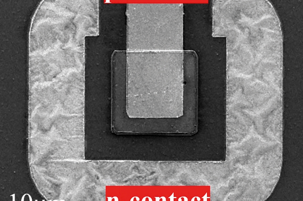
Yao and co-workers produced a range of deep-UV microLEDs by taking AlN-on-sapphire templates, loading them into an MOCVD reactor, and depositing heterostructures that feature four 1.5 nm-thick quantum wells, a 5 nm-thick magnesium-doped electron-blocking layer and a 40 nm-thick short period superlattice. Square microLEDs with sides either 300 µm, 80 µm, 40 µm or 20 µm in length were produced by using reactive ion etching to create mesas. These devices are equipped with a semi-reflective p-type contact and a 50 nm-thick SiO2 passivation layer, added by atomic-layer deposition.
Measurements on a subset of microLEDs emitting at 277 nm show that increasing the mesa width from 20 µm to 300 µm results in an increase in forward voltage from 7.6 V to 9.1 V. This is attributed to improved current spreading in the n-AlGaN layer – although there is also a small effect due to increased current leakage.
Additional studies on deep-UV LEDs with emission wavelengths of 291 nm and 304 nm, realised by adjusting the AlGaN composition in the quantum wells, followed the trend of smaller devices delivering a higher external quantum efficiency at the drive current of 20 A cm-2.
The 304 nm microLED with a side of 20 µm produced the highest peak external quantum efficiency within the study, hitting 4 percent during on-wafer measurements. The picture above shows a scanning electron microscopy image of a deep-UV LED produced by UCSB that has dimensions of 20 µm by 20 µm.
Since reporting these results, the team has realised an external quantum efficiencies of around 5 percent on bare chips with similar structures, produced using a similar fabrication process. Hitting 5 percent is significant, as it is as high as the best commercial deep-UV LEDs, according to Yao. “But all of them are fully packaged, thin-film flip-chip bonded and transparently encapsulated on a reflective header, which we currently lack the expertise in.”
Based on conversations with UV LED vendors, the team expects that the introduction of full packaging will roughly double the output power of their devices.
As well as reporting their better, more recent bare-wafer results, the team plans to incorporate additional structures into their deep-UV emitters, such as array of microLEDs with common contact. This will enable devices to combine a high external quantum efficiency with a high absolute power.
Reference
Y. Yao. et al. Appl. Phys. Express 15 064003 (2022)


