New SiC Epitaxy Substrate Prep Solution from Oxford Instruments

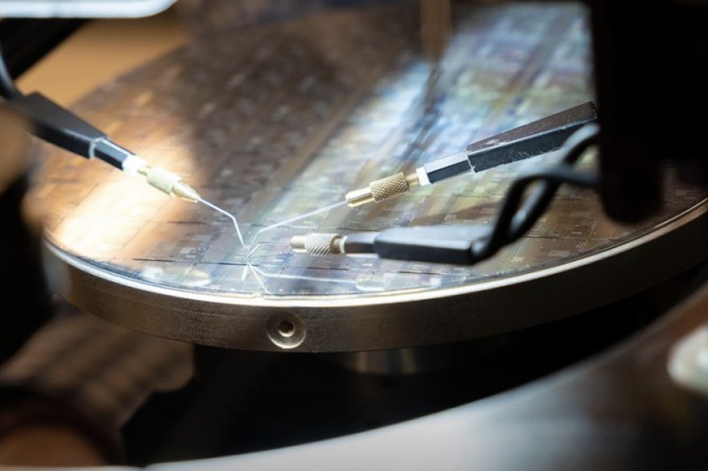
Oxford Instruments Plasma Technology has announced a new alternative method of preparing SiC substrates for epitaxy. Plasma polishing for SiC substrates has been demonstrated as a superior and HVM compatible alternative to Chemical Mechanical Planarization (CMP), while alleviating significant technical, environmental and supply-chain issues associated with CMP.
The Oxford Instruments’ Plasma Polish Dry Etch (PPDE) process is a direct plug and play replacement for CMP and easily integrates into existing process flows. CMP has been the process of record for SiC substrate preparation for many years, but suffers from undesirable operational issues and the industry as a whole is struggling to meet increasing demand for SiC substrates. Operating CMP in SiC substrate fabs has a large environmental footprint due to the semi-toxic slurry biproduct, and the heavy water usage that the process demands is wasteful. In addition, the polishing pads and speciality chemicals bring significant consumable cost in a challenging supply chain environment. Furthermore, the CMP process is inherently unstable as slurry chemicals and polishing pads are consumed, introducing drift into the process line. PPDE is a stable non-contact process, which reduces handling loss and allows for the processing of thinner wafers and producing more wafers per boule.
“There is a compelling technical and commercial case for choosing plasma surface preparation to produce epi-ready SiC substrates. From a technical perspective we have a route to thinner wafers with less bow and excellent epi-ready quality, a strong commercial case for taking cost and complexity out of the supply chain, in addition to providing a significantly cleaner greener process that is fab compatible and integratable” comments Klaas Wisniewski, Plasma Technology’s Strategic Business Development Director, who also added: "This is an incredibly attractive proposition that, as a technique compared to the current method, provides better results at lower cost, drops into the production flow like for like, and enables environmentally sustainable production of SiC devices.”
Oxford Instruments Plasma Technology will formally launch their PPDE process at the International Conference on Silicon Carbide and Related Materials (ICSCRM / ECSCRM), in Davos Switzerland 11-16 September 2022. In the conference technical sessions, they will present their latest whole wafer epi and device results utilising their patented PPDE process, from wafers manufactured by their commercial foundry partners. There will also be an opportunity to speak in person at the event to discuss implementing PPDE in high volume manufacturing fabs.
Register to attend at this link https://icscrm2022.org/registration and to prearrange an in-person meeting, contact Brian.Dlugosch@oxinst.com (VP, strategic production markets, Oxford Instruments Plasma Technology).


