Oxford Instruments validates Alternative to CMP
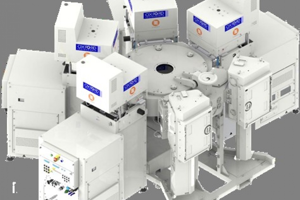
Company completes feasibility study at SiC fab of SiC plasma epi prep alternative to CMP
Following Oxford Instruments announcement of its plasma alternative to CMP product, being launched at the International Conference on SiC and Related Materials (ICSCRM / ECSCRM) in Davos Switzerland on 11-16 September 2022, the company is sharing further news.
Oxford Instruments' non-contact plasma etch method of preparing SiC substrates for epitaxy delivers comparable results to CMP but with lower OPEX, higher device yield and a process window capable of supporting the transition to thinner wafers and therefore increasing wafers per boule.
In a feasibility project, carried out at a tier 1 SiC semiconductor manufacturing fab using whole wafers, the company found that performance of the new plasma substrate preparation technique is already equivalent to CMP for epitaxy readiness.
"This validation outcome is a significant milestone in our goal of creating a more cost-effective and sustainable technique for preparing SiC substrates for epitaxy" comments Klaas Wisniewski, Plasma Technology’s strategic business development director, who also added: "Our Plasma epi-prep technology is hugely promising and currently compares favourably to existing alternatives, but has the potential to exponentially increase substrate production and meet the growing demand for SiC substrates in high growth markets."
Oxford Instruments will formally launch the plasma epi-prep solution at the ICSCRM, in Davos Switzerland 11-16 September 2022. In the conference technical sessions, the company will present their latest whole wafer epi and device results utilising its patented dry etch process.
There will also be an opportunity to speak in person at the event to discuss implementing plasma epi-prep in high volume manufacturing fabs.


