
Tokyo team makes thin seams of light with TMDCs
Four different TMDCs enabled the creation of six different types of sharp, atomically thin 'seams'
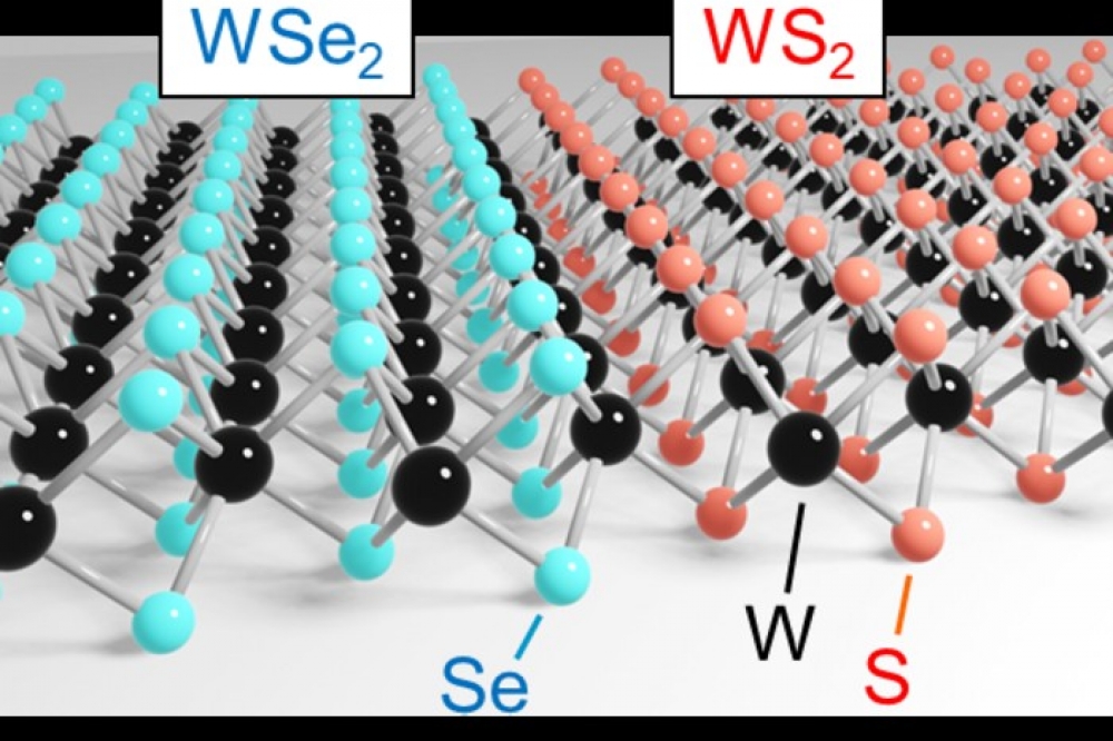
Researchers from Tokyo Metropolitan University have developed a way to produce high quality monolayers of a selection of different transition metal dichalcogenides (TMDCs) which meet over an atomically thin seam.
By coating this layer with an ion gel, they could excite light emission along the seam. The light was also found to be naturally circularly polarised, a product of the customisable strain across the boundary.
LEDs are ubiquitous but there is still a need for even more power efficient solutions. One option involves the application of in-plane heterostructures, where ultra-thin layers of different materials are patterned onto surfaces to produce boundaries. In the case of LEDs, this is where electrons and holes recombine to produce light.
The efficiency, functionality, and scope of applications for such structures are determined not only by the materials used but by the dimensions and nature of the boundaries, which has led to a great deal of research into controlling their structure at the nanoscale.
A team of researchers led by Yasumitsu Miyata of Tokyo Metropolitan University have been using CVD to controllably deposit elements onto surfaces to create atomically thin monolayers. Much of their work has been to do with how such monolayers can be varied to create patterns with different regions made of different TMDCs.
Now, the same team have succeeded in refining this technology. They've redesigned their growth chamber so that different materials could be moved closer to the substrate in a set sequence. They also introduced additives to change the vaporisation temperature of each component, allowing for optimised conditions for the growth of high-quality crystalline layers.
As a result, they succeeded in using four different TMDCs to create six different types of sharp, atomically thin 'seams'. Furthermore, by adding an ion gel, a mixture of an ionic liquid (a fluid of positive and negative ions at room temperature) and a polymer, a voltage could be applied across the seams to produce electroluminescence, the same basic phenomenon underlying LEDs. The customisability of their setup and the high quality of their interfaces makes it possible to explore a wide range of permutations, including different degrees of strain between different TMDCs.
Interestingly, the team discovered that the boundary between a monolayer of WSe2 and WS2 produced a handed form of light known as circularly polarised light, a direct product of the strain at the seam. This new degree of control at the nanoscale opens up a world of possibilities for how their new structures may be applied to real devices, particularly in the field of quantum optoelectronics.
Reference
'Efficient and Chiral Electroluminescence from In-Plane Heterostructure of Transition Metal Dichalcogenide Monolayers' by Naoki Wada et al; Advanced Functional Materials 08 July (2022)


