
Finwave: getting GaN ready for 5G
Can a relatively unknown MIT spin-off deliver the fast, cheap GaN finFETs that an entire industry needs? Finwave co-founders, Bin Lu and Tomas Palacios, have teamed up with industry veterans from International Rectifier, Peregrine Semiconductor and Soitec to do just this, reports Rebecca Pool.
Come 2025, 5G networks are likely to cover one third of the world population accounting for some 1.2 billion connections, predicts the GSMA, UK's Global System for Mobile Communications. The impact on the mobile industry will be profound, a fact that hasn't been lost on many a semiconductor start-up vying to provide the tech the telecoms industry needs to chase ever-higher speeds and efficiencies.
One clear example is US-based Finwave Semiconductor, the MIT spin-off that started life as Cambridge Electronics and following a decade of quiet development, has emerged and rebranded to commercialise its high efficiency, high linearity GaN devices. Announcing its intention to 'revolutionise the future of 5G communications' in June this year, Finwave has also just won $12.2 million in Series A funding to expand its team, ramp up product development and get its FinFET-based GaN transistors swiftly to market.
As lead financier, Jennifer Uhrig, from Fine Structure Ventures, said at the time: “Finwave's technology unlocks the promise of 5G... The company combines best-in-class power amplification efficiency with high-volume manufacturing to overcome the performance and cost limitations that have together stymied widespread adoption of mmWave.”
Firm foundation
The fin field-effect transistor (FinFET) - with its multiple-gate architecture and nanometre-sized fin-shaped channels - isn't new. Thanks to superior gate control and reduced short-channel effects, silicon FinFETs have been widely used in digital and memory applications as CMOS technology nodes have shrunk over the last decade.
However, at the same time, researchers worldwide have also developed GaN FinFETs for high voltage, high frequency RF and power applications, with GaN-on-silicon FinFETs emerging more recently. And this is where, at least for 5G, the technology holds huge appeal.
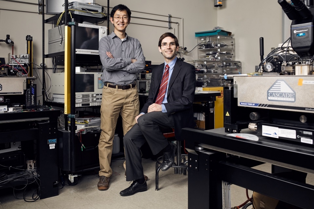
As Bin Lu, Finwave's chief executive and co-founder, points out, the 3D fin structure was exactly what GaN transistors needed to raise efficiency and linearity, to meet 5G requirements. “We started to work on GaN-on-Si devices at MIT back in 2007, and then decided to borrow the silicon FinFET architecture and bring this to GaN so we could really shrink the gate length of the transistor,” he says. “On doing this, we discovered some unique things about GaN FinFETs, including the reduced short channel effect and improvements in transistor linearity.”
During this time, Lu and colleagues also devoted much time and effort to manufacturability, initially fabricating structures on 1 cm2 coupons and pioneering their so-called etch-stop barrier structure to progressively scale up the technology to 6 inch and 8 inch Si CMOS fabrication. Since Autumn 2021, with the support of the ARPA-E SCALEUP (Seeding Critical Advances for Leading Energy technologies with Untapped Potential) program, they are working with industry's key epitaxial wafer vendors and partners in an industry first, to transfer their FinFET process to a US-based 8 inch silicon wafer manufacturing plant.
Industry experience
From word go, Lu has worked closely with fellow company co-founder Prof. Tomas Palacios but in the last year or so, they have been joined by key industry veterans. Jim Cable, past chief executive of RF SOI pioneer, Peregrine Semiconductor, is chief strategy officer, while Ian Warbrick, also from Peregrine and International Rectifier, holds the position of chief operating officer. Thom Degnan, past Soitec, US, president and chief operating officer as well as Intel, Infineon and Qualcomm vice president, also stands as executive vice president of sales and marketing.
Each is excited to be a part of Finwave, has a wealth of experience in manufacturing expansions and in taking new products to market. As Cable puts it: “This journey is similar to past journeys - we're bringing a new material into high volume markets.” And according to Degnan: “We've taken a very organised, ready-aim-fire approach – we've established the value proposition, built the plan and executed that plan – this is a very good team.”
Going forward, Cable believes the company's 8 inch and eventually 12 inch CMOS compatible processes - which don't require any special tooling - are going to be critical. Following their GaN FinFET on an 8-inch R&D process, they now expect to qualify 8 inch volume production by the middle of next year.
“The biggest cost reduction comes from using CMOS foundries.... and our thrust is to really get eight inch GaN into high volume production,” highlights Cable. “Today, it is a challenge for epi-growers to do 12 inch GaN-on-silicon – but there are people that have done this.”
All executives agreed that the transition will only come once the market can support 12 inch volumes. Still, as Cable adds: “Soitec has invested in our Series A round of funding, and is the best materials company in the world. [Twelve-inch] is going to happen, there is no fundamental reason why it can't, and I think we could demonstrate it by the end of next year.”
For his part, Lu believes that now is absolutely the right time to be taking GaN-on-silicon FinFET transistors to market with the necessary linearity improvement and cost reduction. “As we go to 5G, everyone is looking for technologies that can be more linear,” he says. “GaN-on-silicon is coming, it's going to dominate RF devices at volume, and we've got the key technology to do this.”


