
Aixtron launches next gen SiC Epitaxy system
G10-SiC 200 mm system targets volume manufacturing of latest generation SiC power devices
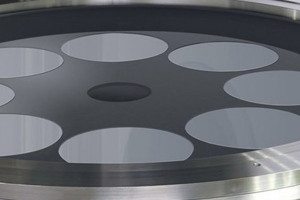
Aixtron SE has launched its new G10-SiC 200 mm system for high volume manufacturing of latest generation SiC power devices on 150/200 mm SiC wafers.
This high temperature CVD system was announced at the International Conference on SiC and Related Materials (ICSCRM), currently taking place in Davos, Switzerland.
The new G10-SiC system is built on the established G5 WW C 150 mm platform and provides a flexible dual wafer size configuration of 9x150 and 6x200 mm. This feature is instrumental for the transition of the SiC industry from 150 mm (6 Inch) to 200 mm (8 Inch) wafer diameter.
The new platform is built around Aixtron's automated wafer cassette-to-cassette loading solution with high temperature wafer transfer. Combined with high growth rate process capabilities, the G10‑SiC is said to provide best-in class wafer throughput and throughput per square meter to efficiently use the limited cleanroom space available in semiconductor fabs.
The Aixtron G10-SiC supports a large variety of device structures incl. single and double drift layer structures meeting stringent 150 mm uniformity requirements of sigma values less than 2 percent for doping and thickness. The automated wafer loading reduces the risk of particle defects to a minimum, resulting in typical defect counts of < 0.02/cm2.
“This is a truly new generation high-performance system. The new dual wafer size configuration fully supports the transition from today’s 150 mm wafer technology and safeguards the investments of our customer for the future. With the highest throughput available to date in this form factor, it maximises fabs productivity and capability to ramp even faster”, says Dr. Frank Wischmeyer, VP SiC of Aixtron. At the same time, the newly developed in-situ top side wafer temperature control (TTC) solution optimises the wafer-level process control within a batch as well as from batch-to-batch. This results in predictable high yields meeting tight production specifications at competitive cost levels”, adds Wischmeyer.
Epitaxial layer uniformity is essential to meet a high yield on device level. The high throughput of the system paired with low consumption costs per processed wafers results in the lowest cost per wafer in the industry, according to the company.
“We are proud to deliver yet another solution to our partners around the globe, that combines industrial top-standard and immense climate effects. The positive feedback from our partners and customers after evaluation and production qualification of our new G10-SiC system has already generated additional customer interest”, says Felix Grawert CEO & president of Aixtron SE.
“The G10-SiC is becoming an important building block for our customers’ worldwide production expansion, and we are committed to support this scaling with our system manufacturing, service and process support excellence.”, Grawert concludes.


