

BluGlass’ Silicon Valley fab up and running
Facility is now operational with development and manufacturing commencing
Semiconductor developer BluGlass has announced that its Silicon Valley production fab now has several operational manufacturing processes for GaN laser diode development and is contributing to the company’s technical roadmaps.
GaN wafers shipped from BluGlass’ Silverwater (New South Wales) facility have commenced front and back-end processing steps in the Silicon Valley fab, complementing and accelerating the company’s contract manufacturing development.
The fab is also being used for short-loop development cycles, enabling BluGlass to test iterations of the key components of laser diodes – metals, facets, and bonds - without requiring a full product. These in-house short- loops can be completed many times faster than processing cycles through contract manufacturers.
BluGlass’ Silicon Valley production fab has now been awarded all requisite regulatory approvals, including Environment Protection Authority (EPA), air quality, and waste management permits.
Jim Haden, BluGlass president, said: “Successfully bringing a semiconductor manufacturing fab online and up-to- speed in a new material class is an important milestone. Our captive fab is now contributing to our technical roadmaps, enabling us to speed product development while also reducing our cost base.
“By bringing core fabrication processes in-house, we reduce supply chain complexity and improve the quality and consistency of our laser diodes. Each process we bring in-house is the equivalent of a specialist supplier being integrated into the business - reducing the complexity of co-ordinating efforts and problem-solving at multiple locations.”
BluGlass is steadily progressing towards commercial reliability with its 405nm and 420nm single and multi-mode devices.
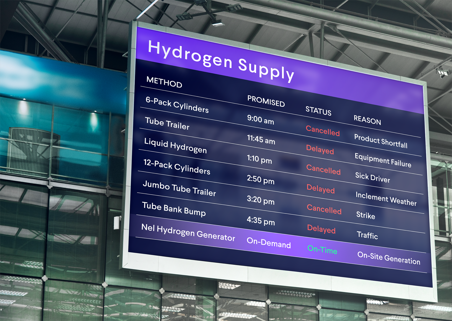
Secure Your Hydrogen Supply
A study supply of high-purity hydrogen is critical to semiconductor fabrication. Supply chain interruptions are challenging manufacturers, leading to production slowdowns and stoppages. On-site hydrogen generation offers a scalable alternative for new and existing fabs, freeing the operator from dependence on delivered gas.Plant managers understand the critical role that hydrogen plays in semiconductor fabrication. That important job includes crystal growth, carrier gas, wafer annealing, and in the emerging Extreme UV Lithography (EUV) that will enable new generations of devices. As the vast need for semiconductors grows across all sectors of world economies, so does the need for high-purity hydrogen.
Take control with Nel on-site hydrogen generation.
Read more