
Co-doping promises ultra-efficient white Ga2O3 LEDs
Ga2O3 LEDs with rare-earth ions have a high colour rendering index while avoiding the losses associated with the Stokes shift
The tremendous success of today’s white LEDs should not obscure their weaknesses. The common architecture, the pumping of a yellow phosphor with a blue-emitting chip, leads to several drawbacks, including a low colour-rendering index, a Stokes energy-converting loss and reduced thermal stability.
Switching from phosphors to rare-earth ions should eradicate these weaknesses, with recent success on this front reported by a team from Saga University. It is pioneering Ga2O3 LEDs that are co-doped with tantalum, europium and erbium ions.
Spokesman for the team, Qixin Guo, told Compound Semiconductor that the nature of the energy transfer mechanism in their co-doped, gallium oxide LEDs, which colour-mix emission from the red, green and blue, requires further investigation. “However, there are no losses due to the Stokes shift.”
The team’s latest emitters build on previous efforts at developing Ga2O3 LEDs with rare-earth ions. Back in 2021, Guo and co-workers reported a white-emitting LED containing a vertical stack of 150 periods, comprising films of Ga2O3 doped with either tantalum, europium or erbium.
As a complicated deposition process is required to produce an LED with so many layers, the team has moved on to investigate the feasibility of colour-tuneable LEDs based on co-doped tantalum, erbium and europium. Their device, formed by uniting co-doped Ga2O3 with a p-type GaAs heterostructure, has a threshold voltage of around 9 V and emits coloured electroluminescence.
To produce their devices, Guo and co-workers employed a pulsed laser deposition tool to grow a Ga2O3 film that is co-doped with tantalum, erbium or europium on p-type GaAs (111). For this process they used a substrate temperature of 500 °C, a growth pressure of 0.1 Pa, an oxygen atmosphere, a growth time of 3 hours, and a distance between the substrate and the target of 40 nm.
“Laser deposition is suitable for fundamental research,” remarked Guo, but added that MOCVD offers the best method for mass production.
Scrutinising their LED structure with X-ray diffraction and Raman spectroscopy revealed that the co-doped Ga2O3 film is polycrystalline, and suitable for producing an LED.
Measurements of the device, made by sputtering a 250 nm-thick film of ITO on the surface of Ga2O3 and adding a gold electrode to the backside of the wafer by electron-beam evaporation, showed that no emission is observed under reverse bias. Its absence indicates that device operation requires simultaneous injection of electrons and holes.
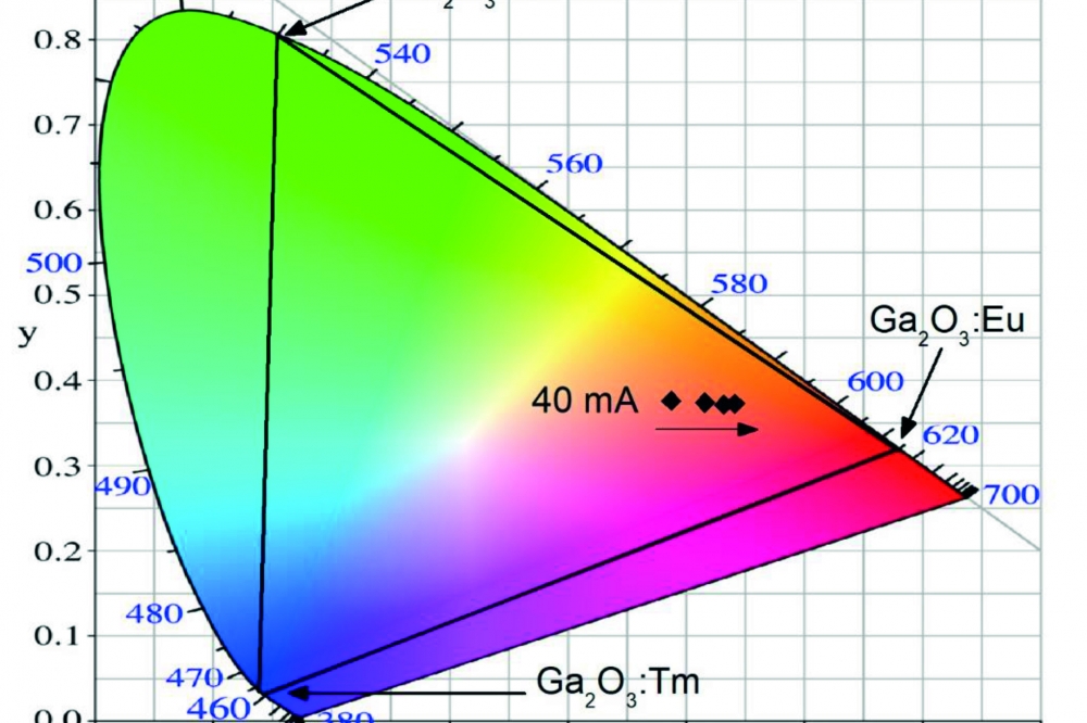
The combination of the tantalum, erbium and europium ions – said by Guo to be the optimal dopants for making a white LED – produces sharp emission peaks at around 460 nm, 530 nm and 610 nm, respectively. This led to bright, uniform pink light that gradually shifts in colour with drive current.
According to the team, white light can be realised with the existing combination of rare-earth ions by fine-tuning the doping concentrations of tantalum, erbium and europium.
One of the strengths of the co-doped Ga2O3 LED is that its emission wavelength does not change with the ambient temperature.
Guo and co-workers are still to investigate the efficiency and lifetime of their LEDs. Neither, though, are next on the agenda. Instead, efforts are now going to be directed at low-temperature photoluminescence measurements, to reveal the energy transfer mechanism with co-doped gallium oxide films.
Reference
Y. Huang et al. Appl. Phys. Express 15 081005 (2022)


