
World's first inverted gallium oxide DI-MOS transistor
Novel Crystal Technology confirms major progress in development of gallium oxide power transistors
Japan-based Novel Crystal Technology has confirmed the basic operation of a high-breakdown voltage (1 kV) gallium oxide inverted double implanted MOS transistor (DI-MOSFET) with a sufficiently high threshold voltage of 6.6V. This is believed to be a world's first for gallium oxide (B-Ga2O3).
The details on this development were announced at the 83rd Japan Society of Applied Physics Autumn Meeting Symposium on September 21, 2022.
Novel Crystal Technology has been aiming to commercialise the B-Ga2O3 transistor since 2019 by participating in the ‘Research and Development of Inverted MOS Channel Type Gallium Oxide Transistor’ program of the National Security Technology Research Promotion Fund (JP004596) of the Japanese Acquisition, Technology & Logistics Agency.
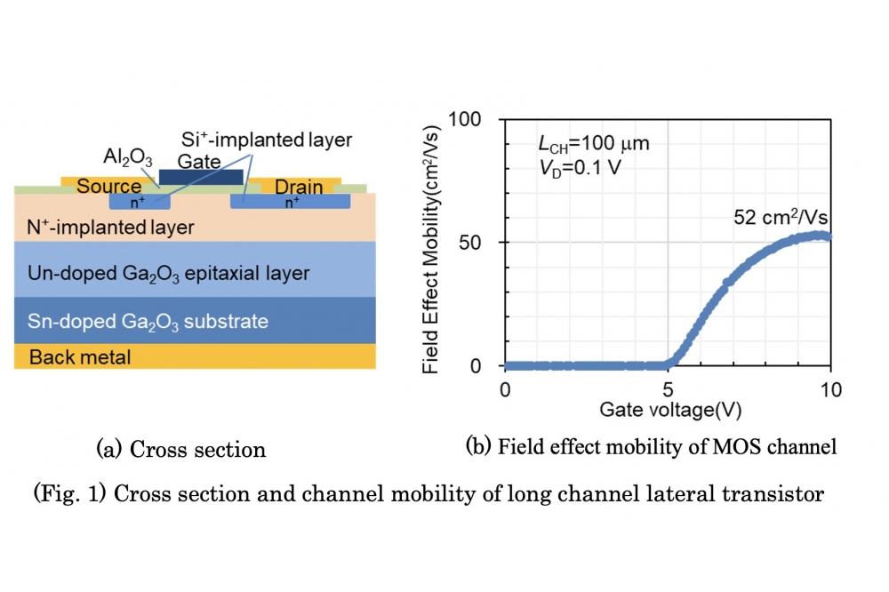
Until now, normally-off B-Ga2O3 transistors have used a fin structure that does not require a p-type layer because the p-type conductive layer technology has not yet been established. However, the fin must have a fine structure of 0.4 μm or less with good dimensional control. It has been difficult to fabricate large devices such as this with a chip size of several millimeters square with good yield.
In response to this problem, Novel Crystal Technology, Inc. has been developing an inverted MOS channel structure that can be manufactured with high yield even using conventional stepper exposure equipment and dry etching equipment. Instead of relying on developing the technically challenging B-Ga2O3 p-type conductive layer, the current development uses a high-resistance B-Ga2O3 layer doped with nitrogen (N) as an acceptor impurity and a well layer made through an activation heat treatment.
In a mobility evaluation, the fabricated long-channel (LCH=100 μm) lateral transistor exhibited a high threshold voltage of 6.2 V, which could not be achieved with a fin structure, and a higher MOS channel mobility (52 cm2/Vs) than that of a device made from SiC (Fig. 1 above).
Novel Crystal Technology, Inc. will analyse the characteristics of the N-doped B-Ga2O3 high-resistance layer in the prototype inverted MOS transistor as part of the project commissioned by the Acquisition, Technology & Logistics Agency. In addition, it will conduct trial production on a 4-inch mass production foundry line, improve the device characteristics, and ensure reliability.
It will also proceed with the development of a full B-Ga2O3 power module combined with a gallium oxide Schottky barrier diode (SBD) that is now being commercialised.


