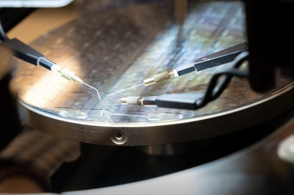
Quashing droop with cubic GaN
Cubic GaN combats droop through elimination of internal electric fields and a reduction in the effective hole mass.
BY YI-CHIA TSAI, JEAN-PIERRE LEBURTON AND CAN BAYRAM
FROM
THE UNIVERSITY OF ILLINOIS AT URBANA-CHAMPAIGN
1962 marked a significant milestone in LED development. That was the year that the late Nick Holonyak Jr. invented the world’s first visible LED, emitting in the red, making the prediction that this class of device would go on to be the most efficient form of lighting ever created.
An important step towards this goal came three decades later, through the introduction of a practical blue-emitting source, based on InGaN. Since then it might feel that we are tantalisingly close to enjoying the ultimate form of solid-state lighting, involving colour mixing of efficient, direct-emitting red, green and blue sources. But this dream is yet to materialise, as a high-performance green LED is still elusive.
At first glance, this ultimate solution may not actually seem to be that important any more. After all, the world has now, by and large, ridden itself of the incandescent bulb, an inefficient, unreliable source that converted 90 percent of electricity into heat. But one should certainly not be complacent. According to the Global Lighting Challenge, lighting still accounts for 15 percent of the world’s electricity consumption and 5 percent of all greenhouse gas emissions. And this situation is only expected to deteriorate, with research from Moira Zellner’s group at Northeastern University forecasting a tripling of the average household energy consumption for lighting over the next fifty years, due to population growth and an increase in housing size. Due to this, there is much urgency to transition to more-energy-efficient lighting, as this will play a key role in curbing carbon footprints.
At the heart of today’s solid-state lightbulbs are a battalion of InGaN-based LEDs, each with an active region made of InGaN quantum wells (QWs), interlaced with GaN quantum barriers. This active region is sandwiched between n- and p-doped GaN layers. The other key ingredient in this heteroepitaxial stack is an AlGaN electron-blocking layer. Sitting between the active region and p-doped GaN, it is included to prevent electrons from spilling over into the p-type region (see Figure 1 for a diagram of the LED).
Figure 1. (a) An InGaN-based LED structure. (b) Competing mechanisms in
an InGaN-based LED. (c) The efficiency droop in traditional blue and
green LEDs.
In this standard form of LED, which operates under forward bias, electrons and holes are driven towards the QW active region, where they recombine to emit light. However, this is a gross simplification of what is really taking place, with carrier transport actually governed by multiple processes, including the quantum-confined Stark effect (QCSE), radiative recombination, Shockley-Read-Hall recombination, Auger recombination, carrier leakage, and a number of magnesium-related processes (for an illustration of all these phenomena at play, see the bottom-left diagram of Figure 1).
The result of all these effects is efficiency droop, a malady behind the peaking of external quantum efficiency at low current densities (less than 35 A cm-2) and its roll-off under high injection levels (see the right sub-figure of Figure 1). Droop is clearly highly undesirable, imposing a trade-off in traditional solid-state sources between the output power of the light source and its efficiency and cost.
LED droop: Inevitable or avoidable?
Much effort has been directed at uncovering the origin of efficiency droop in InGaN-based LEDs. Success is not easy, because it is challenging to isolate each non-radiative mechanism experimentally. Numerous culprits have been proposed – they include, but are not limited to, Auger recombination, carrier leakage, internal polarization and phase-space filling. However, none explains efficiency droop alone.
In some of the latest experimental works, hot-carrier emission from the active region of an InGaN-based LED strongly points to Auger recombination. But there are other experiments that have led researchers to attribute the mixture of mid-energy and high-energy peaks in the electron emission spectra to the coexistence of secondary Auger-electrons escaping the quantum wells and carrier leakage in InGaN-based LEDs.
Can theoretical studies clear up this matter? Well, not yet. Some simulations show that the Auger current outweighs the carrier-leakage current in InGaN-based LEDs, where phonon scattering, alloy scattering, and interface roughness scattering are proposed to explain a large Auger coefficient of 10-30 cm6 s-1. But this explanation is inconsistent with the low efficiency droop in GaAsP-based LEDs, which have similar Auger coefficients.
There are also simulations that point to carrier leakage. They show that efficiency droop and carrier leakage diminish when either: crystal growth is switched to non-/semi-polar substrates, there is an increase in barrier doping, or the electron-blocking layer is designed to have an internal polarization match to the substrate. Support for this view comes from remedies against efficiency droop that have been shown to trim carrier leakage. However, as effects on Auger recombination have not been investigated simultaneously, there is the possibility of misinterpretation of the inherent cause of droop. To try and get to the bottom of this matter, our team at the University of Illinois at Urbana-Champaign developed a new quantum-corrected drift-diffusion LED simulator called the Open Boundary Quantum LED Simulator, shortened to simply OBQ-LEDsim.
Our simulator has enabled us to demystify the interplay between Auger recombination, carrier leakage, and internal polarization, as well as their respective contributions to efficiency droop. It is important to note that, compared with conventional LED simulators, OBQ-LEDsim solves the Schrödinger equation by variational principles, where the ground-state wavefunction vanishes at infinity. While perfectly consistent with the conventional k·p method, our variational approach has the advantage of removing artificial boundaries between the quantum well and classical continuum. This provides high-accuracy modelling of both the inter-QW carrier interaction and QW carriers at arbitrary positions outside of the wells. Thanks to this capability, our OBQ-LEDsim model captures non-radiative processes outside the active region that potentially contribute to efficiency degradation.
A common, simple way to describe the internal quantum efficiency of an LED is the ABC model. That assumes carrier symmetry – i.e. the electron density is the same as the hole density. Under this assumption, the measured Auger coefficient, called the ambipolar Auger coefficient (Ca), has a value equal to the sum of the Auger coefficients for the electron-electron-hole (eeh) and the hole-hole-electron (hhe) channels (Ca = Cn + Cp).
Applying this ABC model to piezoelectric materials such as InGaN is questionable, because the carrier symmetry is plagued by internal polarization. Our investigations have revealed that the major culprit of the efficiency droop is the coexistence of a strong internal polarization and a large hole effective mass. The internal polarization leads to a separation of the electron-hole wavefunction, and in turn promotes carrier localization, which degrades radiative recombination but enhances the Auger process.
Compounding the influence of strong internal polarization, there is a large hole effective mass, further enhancing hole localization in the quantum wells. The upshot is that there is a higher hole density than electron density, and thus a larger hhe Auger current compared with the eeh Auger current. With these factors at play, the Auger electron-hole asymmetry value – that is, the ratio of eeh to hhe Auger coefficients (Cn/Cp) – plays a critical role in both the efficiency droop and in quantifying the ambipolar Auger coefficient. Unfortunately, there is a tendency to ignore Auger electron-hole asymmetry in experiments and simulations. When the Auger electron-hole asymmetry increases, it quenches hhe Auger recombination and enhances eeh Auger recombination. Calculations by our team suggest that efficiency droop diminishes from 48 percent to 25 percent as the value for the Auger electron-hole asymmetry increases from 0 to infinity for a current density of 200 A cm-2 and an ambipolar Auger coefficient of 2 × 10-30 cm6 s-1. This decrease in droop indicates that the hhe Auger process is the dominant Auger recombination channel (see Figure 2).
Figure 2. The efficiency droop as a function of eeh (Cn) and hhe (Cp) Auger coefficients under the current density of 200 A cm-2. The ambipolar Auger coefficient (Ca), expressed in units of 2 × 10-30 cm6s-1, is shown as the dotted lines on the colour plot. Multiple solutions for (Cn, Cp) exist for an efficiency droop value.
We attribute this dominance to electrons being less localized than holes in the quantum wells. It is the internal polarization effects, leading to asymmetric carrier distributions that are behind the strong dependence of efficiency droop on the Auger electron-hole asymmetry. Since ambipolar Auger coefficients are commonly extracted via the ABC model that assumes carrier symmetry, the extracted ambipolar Auger coefficients are also subject to carrier asymmetry (i.e. Auger electron-hole asymmetry).
To highlight the influence of Auger electron-hole asymmetry on ambipolar Auger coefficients, we have included in Figure 2 a dashed line that indicates an efficiency droop of 38 percent. We selected this value as a reference, because it assumes Auger electron-hole symmetry and an ambipolar Auger coefficient of 2 × 10-30 cm6 s-1. From the plot, it is clear that there are multiple values of eeh and hhe Auger coefficients that correspond to the same efficiency droop. For instance, for Auger electron-hole asymmetry values that are less than unity, the ambipolar Auger coefficient is smaller than that obtained assuming Auger electron-hole symmetry. Meanwhile, when the Auger electron-hole asymmetry value is equal to zero, the smallest ambipolar Auger coefficient is 1.24 × 10⁻³⁰ cm6 s-1; when the value for the Auger electron-hole asymmetry exceeds 1, the ambipolar Auger coefficient is larger than that obtained assuming Auger electron-hole symmetry; and when the Auger electron-hole asymmetry value is set to infinity, the largest ambipolar Auger coefficient is 5.20 × 10⁻³⁰ cm6 s-1.
According to first-principles calculations, the actual value for the Auger electron–hole asymmetry is around 0.4. Using this figure, we found that the ambipolar Auger coefficient obtained when assuming Auger electron–hole symmetry – consistent with the common, but simple ABC model – is overestimated by as much as 62 percent.
Next phase in LEDs
Our calculations suggest that the coexistence of internal polarization and a large hole effective mass offers an explanation as to why the Auger recombination in traditional hexagonal-phase InGaN-based LEDs is far, far larger than that in GaAsP-based LEDs, despite their similar Auger coefficients. Note that it is not possible to avert the coexistence of internal polarization and the large hole effective mass by modifying the device design or changing the crystal orientation in InGaN-based LEDs, so these are limited levers to addressing efficiency droop. Our view is that there is more to be gained by switching to the cubic phase, which allows the design of InGaN-based LEDs that can combat droop, thanks to the absence of internal polarization and small hole effective masses (see Figure 3).
Figure 3. Tabulated hexagonal- and cubic-phase GaN parameters and the advantages of cubic-phase.
There are many other attributes associated with the cubic-phase of InGaN-based LEDs. Compared to hexagonal-phase GaN, this form of the LED triples hole mobility, halves the magnesium activation energy, offers a higher quantum barrier to the InGaN/GaN quantum wells, and is expected to have a smaller Auger coefficient. The cubic phase is also blessed with a very favourable band structure: there are relatively few energy states close to the conduction band minimum and the valence band maximum, and the energy difference between the first and second conduction bands at the G point is at least 8 eV (see Figure 3). The culmination of all these strengths should allow the cubic GaN-based LED to impede direct and indirect Auger transitions, leading to a smaller Auger coefficient compared with hexagonal cousins.
We have simulated three different forms of InGaN-based LED – conventional hexagonal, non-polar hexagonal, and cubic-phase – because that enables us to single out the effect of internal polarization from the influence of a large hole effective mass on the efficiency droop (see Figure 4). Our results show that in a traditional hexagonal-phase LED driven at 100 A cm-2, droop is as high as 46 percent, due to the coexistence of a strong internal polarization and a large hole effective mass in the structure.
Figure 4. Normalized internal quantum efficiency (IQE) (left y-axis) and
efficiency droop (right y-axis) as a function of current density. Red
open hexagons and blue hollow hexagons refer to the traditional and
non-polar hexagonal-phase LEDs, whereas green solid squares represent
the novel cubic-phase LED.
A significant improvement comes from switching to the non-polar hexagonal-phase, with the crystal orientation perpendicular to the [0001] internal polarization vector. LEDs with this geometry quench internal polarization and have a similar value for hole effective mass to a conventional InGaN-based LED. These changes have led to a reduction in efficiency droop at 100 A cm-2 to 13 percent, due to enhanced overlap of the electron-hole wavefunction and carrier delocalization.
Even greater success comes from the move to the cubic phase. With this class of InGaN-based LED, droop is quashed to just 3 percent, with the reduction in the carrier effective masses delocalizing electrons and holes, and promoting band-to-band radiative recombination. We attribute the minimal droop to the suppression of the internal polarization and a lowering of the hole effective mass – we have assumed the Auger coefficients don’t change. By drawing on our insights, we anticipate that the LED community will invest in cubic-phase InGaN-based LEDs, which will give the green light to a revolution in solid-state lighting.
Figure 5. Cubic GaN epitaxy on large-area (~1 cm2) U-grooved
silicon (100) dies is demonstrated. (Top row) U-grooved silicon (100)
and (middle row) cubic GaN atop. (From left to right) cross-sectional
sketches, top-view photographs, top-view scanning electron microscopy
(SEM) images and cross-sectional view SEM images. (Bottom row) cubic GaN
structural characterization. (From left to right) phase mapping,
tapping-mode atomic-force microscopy and bright-field, top-view,
scanning tunnelling electron microscopy (STEM) images. The plan-view
STEM reveals no threading dislocations or other types of dislocations on
the cubic GaN surface. Stacking faults with a density of 3.27 ± 0.18 x
104 cm-1 are observed.
Final thoughts
Our work follows the footsteps of researchers in the 1990s. Back then efforts focused on direct deposition on cubic substrates, such as GaAs, silicon (100), 3C-SiC and MgO. These foundations plagued cubic GaN with: incredibly high levels of defectivity, which were well beyond 1010 cm-2; structural metastability, such as phase-mixing; and chemical metastability, which included a tendency toward spinodal decomposition. There were also issues arising for chemical incompatibility, such as that with GaAs. Given all these challenges, it’s hardly surprising that cubic-phase InGaN-based LEDs have remained largely unexplored.
Recently, we broke new ground by inventing a novel method for cubic-phase GaN synthesis. Our success draws on the equivalence of the h-crystal <0001> direction and the c-crystal <111> direction. We discovered that if two h-phase growth fronts merge within a degree of around 110° – that is the angle between the two Ga-N bonds in hexagonal tetrahedral bonding – a c-phase will form.
Building on this finding, we have just shown that it’s possible to form areas of cubic GaN with a size of a square centimetre or so via growth on nano-patterned, CMOS-compatible silicon (100) substrates. This enables us to now explore the opportunity for cubic-phase LEDs to address droop and green gap problems in conventional and advanced forms of solid-state lighting.
One should be aware that as well as the LED-related promise of cubic-phase III-nitrides, they have much to offer in other distinguished applications. This class of nitride has great potential in polarization-free photonics, room-temperature ferromagnetism, high-temperature spintronics. It could also serve in normally off transistors and single-photon emitters.
So, in years to come, we may look back on 2022 as the year that started a new, important phase in III-nitrides.
Further reading
- https://www.globallightingchallenge.org/
- A. L. Hicks, T. L. Theis and M. L. Zellner, “Emergent Effects of Residential Lighting Choices: Prospects for Energy Savings,” Journal of Industrial Ecology 19 285 (2015) https://obqledsim.ece.illinois.edu
- Y.-C. Tsai, C. Bayram, and J.P. Leburton, “Effect of Auger Electron–Hole Asymmetry on the Efficiency Droop in InGaN Quantum Well Light-Emitting Diodes,” IEEE J. Quantum Electron. 58 1 (2022)
- Y.-C. Tsai, J.P. Leburton and C. Bayram, “Quenching of the Efficiency Droop in Cubic Phase InGaAlN Light-Emitting Diodes,” IEEE Trans. Electron Devices 69 3240 (2022)
- Y.-C. Tsai, C. Bayram and J.P. Leburton, “Interplay between Auger recombination, Carrier Leakage, and Polarization in InGaAlN Multiple-Quantum-Well Light-Emitting Diodes,” J. Appl. Phys. 131 193102 (2022)
- J. Lee, Y. C. Chiu, M. A. Johar, and C. Bayram, “Structural and Optical Properties of Cubic GaN on U-grooved Si (100),” Appl. Phys. Lett. 121 032101 (2022)
- U.S. Patent 10,027,086 (issued July 17, 2018)


