
Oxford team develops Nanowire assembly process
Approach can pick up single compound semiconductor nanowires and place them with sub-micron accuracy
In a newly-published study, a team of researchers in Oxford University’s Department of Materials led by Harish Bhaskaran, professor of Applied Nanomaterials, describe a breakthrough approach to pick up single nanowires from the growth substrate and place them on virtually any platform with sub-micron accuracy.
The team worked with functional nanowires of InP, AlGaAs, and GeTe on various patterned structures such as electrodes, nanophotonic devices, and even ultrathin transmission electron microscopy (TEM) membranes.
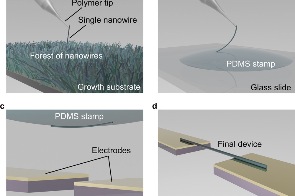
The method uses novel tools, including ultra-thin filaments of polyethylene terephthalate (PET) with tapered nanoscale tips that are used to pick up individual nanowires. At this fine scale, adhesive van der Waals (tiny forces of attraction that occur between atoms and molecules) cause the nanowires to ‘jump’ into contact with the tips. The nanowires are then transferred to a transparent dome-shaped elastic stamp mounted on a glass slide. This stamp is then turned upside down and aligned with the device chip, with the nanowire then printed gently onto the surface.
The figure above shows the nanowire transfer process. a) A single nanowire is picked up by the tapered polymer tip from a forest of nanowires on the growth substrate. b) The nanowire on the tip is placed onto a dome-shaped PDMS stamp cured over a glass slide. c) The stamp with the nanowire is turned upside down and its alignment with the device chip is done under a light microscope. d) Nanowire deposition is completed with the removal of the stamp.
Deposited nanowires showed strong adhesive qualities, remaining in place even when the device was immersed in liquid. The research team were also able to place nanowires on fragile substrates, such as ultra-thin 50 nanometre membranes, demonstrating the delicacy and versatility of the stamping technique.
In addition, the researchers used the method to build an optomechanical sensor (an instrument that uses laser light to measure vibrations) that was 20 times more sensitive than existing nanowire-based devices.
Nanowires, could enable major advancements in many different fields, from energy harvesters and sensors, to information and quantum technologies. In particular, their minuscule size could allow the development of smaller transistors and miniaturised computer chips. A major obstacle, however, to realising the full potential of nanowires has been the inability to precisely position them within devices.
Most electronic device manufacturing techniques cannot tolerate the conditions needed to produce nanowires. Consequently, nanowires are usually grown on a separate substrate and then mechanically or chemically transferred to the device. In all existing nanowire transfer techniques, however, the nanowires are placed randomly onto the chip surface, which limits their application in commercial devices.
DPhil student Utku Emre Ali (Department of Materials), who developed the technique, said: ‘This new pick-and-place assembly process has enabled us to create first-of-its-kind devices in the nanowire realm. We believe that it will inexpensively advance nanowire research by allowing users to incorporate nanowires with existing on-chip platforms, be it electronic or photonic, unlocking physical properties that have not been attainable so far. Furthermore, this technique could be fully automated, making full-scale fabrication of high quality nanowire-integrated chips a real possibility.’
Harish Bhaskaran (Department of Materials) added: ‘This technique is readily scalable to larger areas, and brings the promise of nanowires to devices made on any substrate and using any process. This is what makes this technique so powerful.’
The full paper, 'A Universal Pick-and-Place Assembly for Nanowires', is published in the journal Small.
The work was funded by EPSRC via the Fellowships in Manufacturing (Grant no. EP/R001677/1).


