
HVPE offers a new route to high-quality AlGaN
AlGaN with a vast range of compositions can now be realised by HVPE
Engineers from SCOICS, Japan, claim to have broken new ground by using HVPE to produce high-quality AlGaN layers that span almost all compositions.
By applying growth conditions that enhance etching and suppress parasitic reactions, this team avoids severe surface deterioration, which can arise through microstructural inclusions and the formation of hillocks.
The ability to rapidly grow thick layers of AlGaN promises to improve the production process for a number of devices. For example, the productivity of UV LEDs and lasers emitting in the UV, violet and blue could be enhanced by growing much of the device on GaN or AlN templates coated with thick layers of n-type AlGaN, added by HVPE.
What’s more, SCIOCS technology could open the door to relaxed, n-type, free-standing AlGaN substrates. This could slash the substantial series resistance in UV LEDs and lasers, stemming from the use of n-type AlGaN cladding layers that are very thin, in order to avoid issues associated with the critical thickness. Ensuring a far lower series resistance would deliver a tremendous hike in the output power of UV LEDs and enable CW operation of UV lasers, thanks to suppressed self-heating.
Free-standing AlGaN substrates could also aid wide bandgap HEMTs. This foundation could quash unwanted impurities and address issues associated with device instability.
Note that it’s not possible to reach the growth rates realized by HVPE by simply accelerating MOCVD. The latter technique, widely employed throughout the compound semiconductor industry for chip production, is limited to around 1 µm/hr. Higher growth rates would fail to suppress the vapour-phase reaction, even under low reactor pressures.
The success by SCIOS has drawn on its previous breakthroughs, including the growth of highly pure, highly uniform GaN layers by HVPE. However, using HVPE to extend the growth from GaN to AlGaN is far from easy, according to team spokesman Hajime Fujikura, with efforts stymied by rather complicated chemical reactions. “One needs a huge number of growth trials to reach good results.”
Another barrier to success is the lack of standardisation of HVPE systems. “HVPE systems are completely different from one another,” remarked Fujikura, “so it is very difficult to reproduce HVPE growth results by reading papers from other groups.”
Fujikura believes that the foundation behind the team’s success is the HVPE machine and its accompanying growth technology for producing free-standing GaN, using extreme gas flow-control. “This excellent growth tool is also very helpful for developing good AlGaN growth conditions.”
The engineers from SCIOCS developed their AlGaN technology by studying the growth of this ternary on three different templates: 4 µm-thick GaN on flat sapphire; 0.5 µm-thick AlN on flat sapphire; and 0.5 µm-thick AlN on patterned sapphire, which featured an array of 400 nm-high cones.
Using aluminium, gallium and HCl as starting materials, Fujikura and colleagues produced a range of samples with aluminium fractions spanning less than 10 percent to more than 90 percent, at growth rates typically varying from around 0.1 µm min-1 to 1 µm min-1.
During the study the team found that to ensure a high-quality surface, they had to use etching to supress parasitic reactions. These unwanted reactions might originate from parasitically crystallised AlGaN on the HVPE nozzle and the reactor wall, or from direct nucleation of irregular microcrystals on the epitaxial surface.
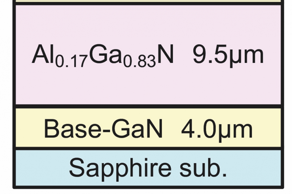
One of the highlights of the work by the team is a 10 µm-thick, fully-relaxed Al0.17Ga0.83N layer with a mirror-like surface, grown on the GaN-on-sapphire template. Its crystal quality is not severely deteriorated by heteroepitaxy, according to X-ray diffraction. Another triumph is a smooth, high-quality layer of Al0.67Ga0.33N, grown on the AlN-on-patterned-sapphire template – this is a promising foundation for realizing UV LEDs with enhanced light extraction.
Fujikura says that the next target is a thick AlGaN layer, which could be used to make free-standing substrates.
Reference
H. Fujikura et al. Appl. Phys. Express 15 085504 (2022)


