
Stretching GaN power devices to 10 kV
GaN power rectifiers and transistors combine a breakdown voltage beyond 10 kV with a specific on-resistance that’s below the SiC limit.
BY YUHAO ZHANG FROM VIRGINIA TECH
One of the keys to getting carbon emissions to net zero is to increase
the efficiency of electrical energy processing. This can be accomplished
through the introduction of semiconductor-based power devices with a
lower on-resistance, a faster switching speed and a high breakdown
voltage.
It is a roll-out that must include devices operating between 1 kV and 35 kV, a range that’s often known as medium-voltage, but also referred to as high-voltage in many contexts. Devices operating in this range are ubiquitously used in electrical grids, renewable energy processing, industrial motor drives and electrified transportation. Driven by this widespread deployment, the market size for medium-voltage power devices has already topped $10 billion and is increasing at pace.

Figure 1. The multi-channel AlGaN/GaN HEMT with a planar gate (a) and a trigate architecture (b).
Dominating today’s medium-voltage power device market are a pair of silicon devices: the insulated-gate bipolar transistor; and the p-n diode, up to a voltage class of 6.5 kV. Both suffer from a slow switching speed, stemming from bipolar operation – as electrons and holes contribute to current conduction, both forms of carrier must be removed or supplied during device switching.
A superior performance can be realised by turning to the unipolar SiC MOSFET and the SiC junction barrier Schottky diode. These alternatives, which enable faster switching speeds, are covering an increasingly broad range of voltages. They have been commercialized up to 3.3 kV, and industrial R&D devices are available up to 10 kV.
But that’s not the ultimate solution, as even better results are possible with SiC’s wide bandgap rival, GaN. Providing a higher critical electric field and a higher electron mobility, GaN enables the fabrication of devices with a lateral or a vertical architecture. Lateral GaN HEMTs operating at up to 900 V are already on the market, and industrial vertical GaN transistors have been demonstrated at the 1.2 kV class. Progress has also been made at far higher voltages. Some groups are reporting GaN devices with blocking voltages close to 10 kV. However, specific on-resistances are much higher than those of SiC counterparts, leading many to conclude that GaN is only advantageous in the low-voltage range.
But those of us at Virginia Polytechnic Institute and State University – better known as Virginia Tech – beg to differ. Working in collaboration with engineers at the University of Southern California, the University of Cambridge, Enkris Semiconductor and Qorvo, we have developed a new generation of lateral medium-voltage devices that are based on a multi-channel GaN platform and outperform their silicon and SiC counterparts.
We produce our devices from multi-channel AlGaN/GaN wafers that consist of vertically-stacked heterostructures, which enable the fabrication of diodes and HEMTs that feature a high mobility two-dimensional electron gas (2DEG) channel. These devices offer a high-power handling capability, thanks to the stacked channels (see Figure 1(a)), and can leverage some of the benefits of vertical devices, such as a spatially distributed current.
By drawing on a series of device innovations we have demonstrated 10 kV GaN Schottky barrier diodes and normally-off HEMTs that exceed the one-dimensional SiC unipolar limit, in terms of the trade-off between the specific on-resistance and the blocking voltage.
Challenges of multi-channel devices
It is easy to understand why the introduction of multiple channels reduces the on-resistance of a device. Using the 4-inch multi-channel GaN wafer grown by Enkris Semiconductor, the devices that we fabricate feature five channels, leading to a sheet resistance of just 120 Ω/sq – that’s about a third-to-a-quarter of that of today’s commercial GaN HEMTs formed from single-channel wafers. The upshot is that a switch to multiple channels enables a dramatic decrease in specific on-resistance.
Unfortunately, enjoying this benefit is far from trivial. There are two fundamental challenges associated with multi-channel devices.
The first arises because when the device is blocking voltage, there is a large volume of charge in the stacked channels that can lead to a fast drop in the electric field. This is a fundamental issue, expected from the simple Poisson equation. Due to this large volume of charge, there is a low average electric field across the device length, and increasing this dimension does not ensure an upscaling of the blocking voltage. Note that with these net charges, even if there is a good edge termination that enables a large peak electric field at the device edge region (see Compound Semiconductor 27 3 44), the blocking voltage of a multi-channel device tends to be much lower than that of a single-channel counterpart with the same length.
The second challenge faced with the multi-channel device is ensuring sufficient gate control. Within a conventional HEMT, a planar gate is often employed to modulate the 2DEG channel. That’s not a good idea in a multi-channel device, because the top 2DEG channel will shield the gate electrostatics from reaching the buried channels. If this approach is taken, there is a very negative threshold voltage, even down to -100 V, and a very poor transconductance. In short, such a device is unsuitable for power electronics applications, which should have devices that are normally off.
A solution to this issue is to turn to either FinFET or trigate architectures, similar to those deployed in deeply-scaled silicon CMOS devices. Introducing a trigate design (see Figure 1 (b)) results in the wrapping of multi-channel fins around a gate stack. With this configuration, the sidewall gate controls the buried 2DEG channels. However, due to the high 2DEG density, the fins must be as narrow as around 10-15 nm to ensure normally-off operation in multi-channel HEMTs. Since today’s power semiconductor industry mainly relies on processing at length scales of 180 nm or more, it is very difficult to manufacture trigate multi-channel HEMTs on an industrial scale.
Reducing the surface field
Complicating the charge profile in a multi-channel architecture is the existence of multiple sources of polarization charge. Overall, a net donor tends to be present, which is in part the origin of the 2DEG in the multi-channel at zero bias. To balance this net donor at high blocking biases, we introduce a p-type GaN cap layer that provides a reduced surface field (RESURF) structure (see Figure 2 (a)). In a diode, this p-GaN RESURF layer extends to near the cathode, and its acceptor charges balance the net donor charges (see Figure 2 (b)). We are able to experimentally realise this charge balance by designing an appropriate p-type doping concentration, or by adapting the p-GaN thickness through a p-GaN etch that is monitored by a test structure.

Figure 2. (a) The p-GaN reduced surface field (RESURF)
architecture improves the performance of the Schottky barrier diode via
charge balancing. (b) Illustration of charge balance at reverse bias.
(c) Forward and (d) reverse current-voltage characteristics of devices
with different anode-to-cathode distances (LAC).
It is worth noting that the addition of this p-GaN cap decreases the 2DEG density, particularly in the top channel. The wafer that we use, provided by Enkris, is produced by MOCVD, with the p-GaN layer grown continuously with the five-channel structure. This has a sheet resistance of 178 Ω/sq, which is still higher than the equivalent wafer without the p-GaN layer. However, compared to the single-channel wafer, the sheet resistance is smaller by more than a factor of two. The upshot is a slight increase in the on-resistance, but this is overshadowed by tremendous gains in blocking voltage, enabled by the RESURF layer.
The introduction of RESURF technology has enabled us to fabricate a Schottky barrier diode with a turn-on voltage of just 0.6 V (see Figure 2(c)), which is lower than that of SiC junction barrier Schottky diodes. Through judicious choice of the anode-to-cathode distance, the blocking voltage of the p-GaN RESURF Schottky barrier diode can be about 1.5-fold higher than that of a Schottky barrier diode with merely a p-GaN termination (see Figure 2(d)).
For RESURF Schottky barrier diodes, the average lateral electric-field can be as high as around 1 MV/cm. This enables a Schottky barrier diode with a 123 mm anode-to-cathode distance to realise a blocking voltage of more than 10 kV and a specific on-resistance of just 39 mΩ cm2 – that’s 2.5-fold lower than the specific on-resistance of state-of-the-art 10 kV SiC junction barrier Schottky diodes.
Normally off 10 kV HEMTs
To realize normally-off operation without the need for sub-micron lithography, we are pursuing a new device concept: the multi-channel monolithic-cascode HEMT, which we refer to as the MC2-HEMT. Due to its cascode configuration, the normally off low-voltage transistor is connected to the normally on high-voltage transistor. The composite that results may be operated in a similar manner to the standalone, normally off, high-voltage transistor. Note that cascode configurations are well established, with commercial devices available in GaN and SiC, where a silicon MOSFET is co-packaged with a GaN HEMT or SiC JFET.
A key difference between these cascode devices and the MC2-HEMT is that the latter builds on a single chip. There is monolithic integration of a low-voltage, normally off HEMT that has a single 2DEG channel and a high-voltage, normally on HEMT that is based on a stacked 2DEG multi-channel (see Figure 3(a)).

Figure 3 (a) The multi-channel monolithic-cascode HEMT, known simply as the MC2-HEMT, combines an on-resistance and blocking voltage that comes from the multi-channel region with a gate control that is dominated by the single-channel region. The design of the MC2-HEMT is shown alongside its equivalent circuit. (b) Transfer characteristics of the MC2-HEMT with and without a gate recess in the low-voltage HEMT. (c) Off-state I-V characteristics of the MC2-HEMT with various lengths of the multi-channel region.
Within this design there is a plurality of Ohmic vias, which function as the effective drain for the single-channel, low-voltage HEMT, as well as the source for the multi-channel high-voltage HEMT. Additional features of this architecture are the introduction of a gate recess in the low-voltage HEMT to ensure normally off operation, and the use of a RESURF structure for the high-voltage HEMT to upscale the blocking voltage.
The MC2-HEMT delivers a strong performance on several fronts, combining an on-resistance and blocking voltage that comes from the multi-channel region with a gate control that is dominated by the single-channel region.
Thanks to these characteristics, our MC2-HEMT can exploit the low sheet resistance that stems from multiple channels while realizing a normally off gate control and enjoying complete shielding of the gate region from a high electric field. This design also obviates the need for sub-micron fin gates, significantly relaxing the lithography requirement.
Measurements of device transfer characteristics (see Figure 3(b)) shows that the introduction of a gate recess to the low-voltage HEMT enables a threshold voltage of over 1.5 V. Meanwhile, off-state current-voltage characteristics (see Figure 3(c)) validate our claim that the blocking voltage scales with the length of the multi-channel region up to more than 10 kV.
For the 10 kV MC2-HEMT, specific on-resistance is only 40 mΩ cm2, which is 2.5-fold smaller than that of 10 kV SiC MOSFETs, and well below the one-dimensional SiC unipolar limit. Another great result for our MC2-HEMTs is that they have the highest Baliga’s figure-or-merit for any power transistors operating at 6.5 kV or more.
Our progress helps to demonstrate that medium-voltage GaN power Schottky barrier diodes and HEMTs operating up to 10 kV will allow GaN power technologies to enter a new era. These devices are breaking ground on many fronts: as well as offering higher voltages, they are setting a new benchmark for the trade-off between on-resistance and breakdown voltage that goes beyond the one-dimensional SiC unipolar limit.
Such results call into question the commonly held belief that SiC is superior to GaN in medium- and high-voltage power electronics. While SiC is now displacing silicon in this power electronic sector, the future surely belongs to GaN.
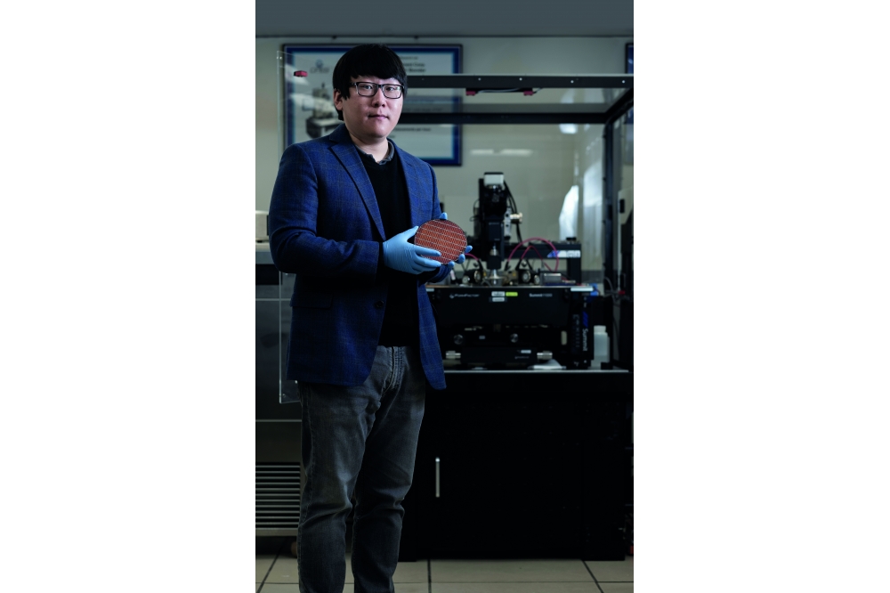
Main Image :Yuhao Zhang holding a GaN power transistor wafer in front of the 10 kV probe station
Further reading
M. Xiao et al. “Multi-Channel Monolithic-Cascode HEMT (MC2-HEMT): A New GaN Power Switch up to 10 kV” 2021 IEEE International Electron Devices Meeting, 5.5.
M. Xiao et al. “10 kV, 39 mΩ·cm2 Multi-Channel AlGaN/GaN Schottky Barrier Diodes” IEEE Electron Device Lett. 42 808 (2021)
Y. Zhang et al. “GaN FinFETs and trigate devices for power and RF applications: review and perspective” Semicond. Sci. Technol. 36 054001 (2021)


