
KnowMade announces GaN newsletter
Patents monitoring company to help clients keep track of GaN developments
Patents monitoring company KnowMade has announced that it will release a monthly newsletter for GaN technology, covering electronics and optoelectronics applications.
KnowMade has been monitoring the GaN scientific and patent landscapes for more than ten years now. The company has witnessed significant growth in activity in both landscapes over the last decade. The number of new patent applications related to GaN technology published in 2019 was more than twice the number of publications in 2015. Today, on average, KnowMade identifies more than 200 scientific papers and more than 250 new patent applications every month related to GaN technology.
KnowMade says that the newsletter will provide a cost-efficient way to detect new players worldwide early on, to access their recent R&D activities and latest collaborations.
Lately, the patenting and scientific activities related to GaN optoelectronics have been partly driven by the development of UV optoelectronic devices, especially deep-UV light-emitting diodes (UVC LEDs), spurred on recently by pandemic demand for disinfection devices. Although several players have made substantial progress and reached the performance and cost specifications of early adopters, there remains a need to significantly improve cost and efficiency for larger market acceptance, driving the publication of numerous related patent filings and scientific works every month.
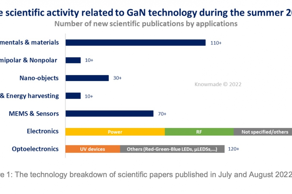
New applications have emerged for GaN LEDs, laser diodes and photodetectors in micro-displays (smart lighting, smart phones/watches, AR/VR in smart glasses, flexible micro-displays, etc.) and visible light communications (for high-speed transmissions in 6G networks, aircraft & underwater communications, communications in hazardous environments, etc.). This is driving the development of new generations of photonic devices and the publication of numerous patents and scientific papers every month with a view to produce high-resolution, high-brightness, GaN-based micro-displays for instance, in a cost-effective way. In the last couple of months, KnowMade identified more than 250 GaN optoelectronics patent applications and more than 120 scientific articles in this field (Figure 1).
GaN power devices have the wind in their sails
Today, GaN technology is well established in RF applications. Scientific and patenting activity regarding RF GaN devices has been slowing down in the last few years. Still, KnowMade identifies about 25 scientific publications every month, most of them from China (≈50 percent) and India (≈20 percent). What’s more, 30 to 50 new RF GaN patent applications are published every month. The domination of Chinese players in the recent patenting activity is even more important seeing as they have published almost 70 percent of the new patent applications every month, far ahead of US, Japanese and European patent applicants (≈30%).
Beyond the improvement and scaling of the current RF GaN HEMT technology, researchers/inventors are investigating new technological ways for future high-power RF electronics, including for instance 3-D GaN nanostructures (e.g., AlGaN/GaN MIS FinFET), alternative substrates (e.g., AlN) and/or epi-structures (e.g., based on N-polar III-nitrides).
Lately, the main driver for the patenting and scientific activities around GaN electronics has been power applications rather than RF applications, with notably more power-related scientific papers and double the number of power-related patents published every month.
Yet the domination of Chinese players in the scientific and patenting activities is once again verified for power applications, with slightly different ratios between Chinese players on the one hand (≈60 percent), and US, Japanese and European players on the other (≈30 percent). However, India does not play as significant a role in either the scientific or patent landscape for power applications as it does in the RF GaN scientific landscape.
Over the last few months, normally-off device structures, especially GaN HEMTs with p-type gate, have been a major focus in the GaN community according to the number of related scientific publications (more than 25 percent of all papers related to GaN electronics). Furthermore, the activities related to GaN vertical devices continue to gain momentum, representing on average over 25 percent of scientific papers and about 10% of new patent publications related to GaN electronics.
Huge GaN markets are opening up
According to market intelligence companies, the power GaN and RF GaN markets are entering a high-growth phase. In optoelectronics as well, there are significant opportunities for GaN technology coming in the next years. The UVC LED market is finally taking off, while the size of the global micro-display market is expected to reach $4.2 billion by 2025 according to Yole Intelligence. On the other hand, the overall visible light communication market is predicted to grow rapidly, at a CAGR of 101 percent over the period 2020-2027, according to Mordor Intelligence. Accordingly, many newcomers are looking forward to positioning themselves in these sizeable markets, thereby challenging the status of historical and well-established players in the different competitive landscapes.


