Loading...
News Article

PragmatIC leads £2.4 million sustainability project

News

Maker of flexible IZGO circuits to accelerate the decarbonisation of semiconductor manufacturing

PragmatIC Semiconductor, a UK company making flexible electronics based on IGZO (In, Ga, Zinc Oxide) TFT semiconductor technology, is leading a £2.4 million project with funding provided by the Made Smarter Innovation: Smart Sustainable Factory Challenge at UK Research and Innovation.

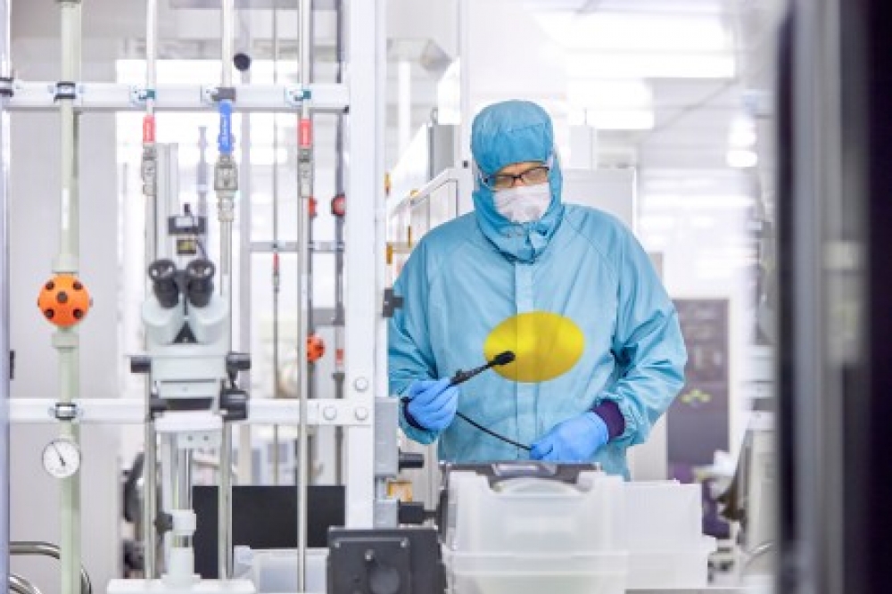
The INSPIRE project will develop and deploy new digital technologies within PragmatIC’s FlexLogIC semiconductor fabrication facilities, to drive improved resource efficiency and reduce the environmental impact of manufacturing operations. To make IGZO FlexLogIC devices, PragmatIC uses a proprietary manufacturing process that deposits layers of IGZO TFTs, resistors and metal layers onto a 200 mm wafer of polyimide.

Specifically, the funding will focus on innovation that will help to accelerate the decarbonisation of semiconductor manufacturing, by optimising the consumption, quality, and recovery of resources across wafer processing, tools, and facilities. The smart factory approaches developed will demonstrate how sustainability can become a measure of fab performance by manufacturers globally.

Scott White, CEO of PragmatIC Semiconductor added “We have already developed semiconductor devices that are significantly more cost-effective and sustainable than traditional silicon chips – and now we are excited to lead the way in new manufacturing technologies that will reduce our environmental impact even further. Ultimately, we aim to develop and define best-in-class sustainable semiconductor manufacturing practices, to accelerate decarbonisation and improve resource efficiency within the industry.”

New manufacturing technologies of interest will include: sensors for capturing resource usage and quality – water, chemicals, gases and energy; AI and machine learning algorithms, aggregating operational, tools and facilities data to drive optimisation; active water and energy management, minimising consumption and maximising recovery; and ensuring operational performance, including measures of capacity, cycle time, equipment performance, process variation and yield improvement.

To realise these aspirations, PragmatIC Semiconductor is working alongside partners such as DevTank, Innoflow and SUEZ.

Commenting on their role in the project, Ben Harding, regional VP for UK and Ireland, SUEZ Water Technologies & Solutions said: “Water scarcity and carbon emissions are issues that impact us on a global scale. INSPIRE is a unique opportunity to apply our 'Insight' digital monitoring platform to measure and optimise consumption, determining best practices for minimising carbon footprint and environmental impact within microelectronics and other manufacturing sectors.”

SPONSOR MESSAGE

Secure Your Hydrogen Supply

A study supply of high-purity hydrogen is critical to semiconductor fabrication. Supply chain interruptions are challenging manufacturers, leading to production slowdowns and stoppages. On-site hydrogen generation offers a scalable alternative for new and existing fabs, freeing the operator from dependence on delivered gas.

Plant managers understand the critical role that hydrogen plays in semiconductor fabrication. That important job includes crystal growth, carrier gas, wafer annealing, and in the emerging Extreme UV Lithography (EUV) that will enable new generations of devices. As the vast need for semiconductors grows across all sectors of world economies, so does the need for high-purity hydrogen.

Take control with Nel on-site hydrogen generation.

Read more
QD company Quantum Science expands into new facility
Innoscience files lawsuit against Infineon
Riber revenues up 5% to €41.2m
Forvia Hella to use CoolSiC for next generation charging
Photon Design to exhibit QD simulation tool
Ortel transfers CW laser fabrication to Canada
Luminus adds red and blue multi-mode Lasers
PseudolithIC raises $6M for heterogeneous chiplet tech
Mesa sidewall design improves HV DUV LEDs
IQE revenue to exceed expectations
'Game-changing' VCSEL system targets clinical imaging
German start-up secures finance for SiC processing tech
Macom signs preliminaries for CHIPS Act funding
IQE and Quintessent partner on QD lasers for AI
EU funds perovskite tandems for fuel-free space propulsion
EU to invest €3m in GeSi quantum project
Transforming the current density of AlN Schottky barrier diodes
Turbocharging the GaN MOSFET with a HfO₂ gate
Wolfspeed launches Gen 4 SiC MOSFET technology
Report predicts high growth for UK's North East
Element Six unveils Cu-diamond composite
SemiQ launches hi-rel 1700V SiC MOSFETs
Lynred to exhibit Eyesential SWIR sensor for machine vision
Thorlabs buys VCSEL firm Praevium Research
Advancing tuneable InP lasers on a heterogeneous platform
P-GaN gate HEMTs have record threshold voltage
Guerrilla RF releases GaN power amplifier dice
Narrow-linewidth DFB lasers now at 405 and 488nm
Researchers develop tech for future fast-charging stations
Vermont GaN Tech Hub awarded nearly $24M
Onsemi completes buy-out of Qorvo SiC JFET business
Quantum Science announces Innovate UK funding
×
Search the news archive

To close this popup you can press escape or click the close icon.
Logo
x
Logo
×
Register - Step 1

You may choose to subscribe to the Compound Semiconductor Magazine, the Compound Semiconductor Newsletter, or both. You may also request additional information if required, before submitting your application.


Please subscribe me to:


You chose the industry type of "Other"

Please enter the industry that you work in:
 
x
Adblocker Detected
Please consider unblocking adverts on this website