
Innoscience extends 650V GaN HEMT family
Company adds190mΩ, 350mΩ and 600 mΩ RDS(on) devices in industry-standard packages
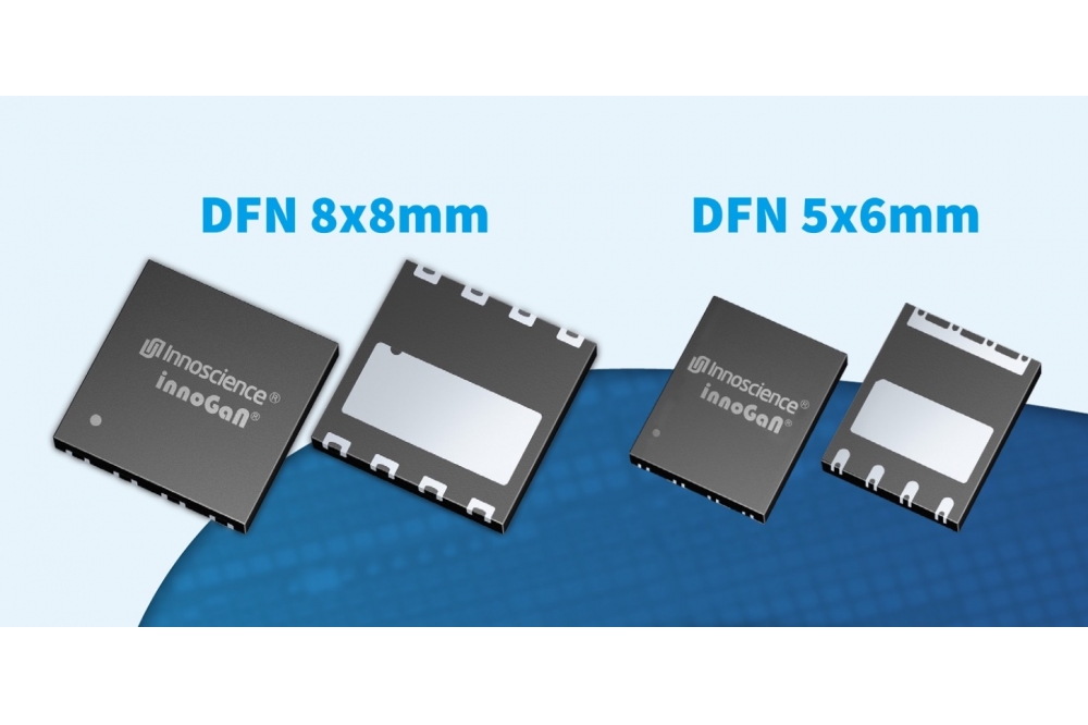
Innoscience has announced a full range of 650V E-mode GaN HEMT devices. New 190mΩ, 350mΩ and 600mΩ RDS(on) devices in industry-standard 8x8 and 5x6 DFN packages join previously-announced 140mΩ, 240mΩ and 500mΩ RDS(on) parts, creating a significant portfolio of available devices.
The 650V HEMTs are qualified to JEDEC standards for chip and package. The devices have also passed Dynamic High Temperature operating life test (DHTOL) reliability testing according to JEP180, which is the newly-released JEDEC’s guidelines dedicated to GaN technology. In addition, Innoscience’s 650V HEMT (InnoGaN) have undergone accelerated life tests beyond 1000V that give lifetime calculations of 36 years at 80 percent of the rated voltage (520V; 150°C; 0.01 parent failure rate).
The new devices also feature very good drain source voltage transient (VDS, transient) of 800V for non-repetitive events with an extended pulse time up to 200µs and a pulsed (VDS, pulsed) characteristics for repetitive pulse up to 100ns of 750V for the 190mΩ RDS(on) parts. These are best-in-class characteristics. Moreover, similarly to the 650V products, the new 190mΩ, 350mΩ and 600mΩ RDS(on) devices all feature a strong ESD protection circuit embedded in the die to ease mass production assembly of these device in package and easy handling.
Possible applications of these new Innoscience devices include PFC converters, DC-DC converters, LED drivers, fast battery chargers, notebook and all-in-one (AiO) adaptors and power supply for desktop PC, TV, power tools, and so on.
Comments Yi Sun, Sr VP of product development at Innoscience: “These new devices complete our 100-600mΩ device portfolio at 650V. I am especially happy to add the 650V/190mΩ, as it is becoming a standard in the GaN industry that offers greater flexibility to customers upon selecting suppliers for their applications.”
Because GaN devices do not have a body diode, reverse recovery losses are much less than silicon MOSFETs and the Figure Of Merit (FOM) is much better. This means that GaN HEMTs, such as Innoscience’s new 650V parts, can be used in simple totem pole configurations for PFC applications, and benefit from the reduced BOM count without incurring the high losses as it would be with conventional Silicon devices. This benefit, combined with the high frequency capabilities of InnoGaN, helps to reduce the size of passives and results in more compact systems.


