
Realising implantation in GaN
Activating magnesium implantation with ultra-high-pressure annealing yields vertical GaN junction barrier Schottky diodes with exceptional performance
Until very recently, there has been a glaring omission from the toolbox of engineers that work with GaN: the absence of an ion implantation process. But that has now been remedied, thanks to a process involving ultra-high-pressure annealing of magnesium dopants, developed by a team from the US and Poland.
According to Dolar Khachariya from Adroit Materials – speaking on behalf of the ground-breaking team that also includes those from North Carolina State University and the Institute of High-Pressure Physics, Poland – the ion-implantation and activation techniques that they have developed for GaN are successful and reliable.
“This technique has allowed us to obtain kilovolt-class-blocking GaN junction barrier Schottky diodes on native GaN substrates,” explained Khachariya, adding that realising even higher blocking voltages is relatively simple, as it just involves increasing the thickness of the GaN epilayer while maintaining the implantation and activation techniques.
Khachariya claims that if GaN-based junction barrier Schottky (JBS) diodes were manufactured by the team’s approach, they would exceed the performance of existing SiC- and silicon-based devices and be significantly more cost-effective.
Although ammonothermal GaN, the ultimate form of bulk GaN, provided the foundation for the work of the researchers, Khachariya said that the same results should be possible with HVPE-grown GaN substrates.
To increase the current capabilities of the diode, larger-diameter devices are required. This is not an issue for GaN substrates grown by the ammonothermal method, because they have dislocation densities in the low 104 cm-2. But Khachariya warned that for HVPE-grown GaN, there is the possibility that large-area devices might not work as intended, due to dislocation densities that are at least two orders of magnitude higher.
Fabrication of the team’s diodes began by loading an ammonothermal n+ GaN substrate into a vertical, cold-wall, RF-heated MOCVD reactor and depositing a 5 m-thick n-type GaN drift layer with a net carrier concentration of around 1.3 x 1016 cm-3. To realise a shallow box profile for implanted magnesium at a concentration of around 2 x 1019 cm-3, the researchers employed a two-step implantation process, involving a tilt angle of 7°, ion energies of 75 keV and 25 keV, and corresponding doses of 2 x 1014 cm-2 and 4.4 x 1013 cm-2, respectively. Subsequent heating of the sample to 1300 °C for 30 minutes at 400 MPa, under a nitrogen gas to prevent decomposition, activated magnesium ions in the sample.
JBS diodes with a 0.1 mm by 0.1 mm device area were formed by adding Ni/Au p-type ohmic contacts, followed by Ni/Au Schottky contacts, to the front of the device, and a Ti/Al/Ni/Au stack to the back side of the substrate. For comparison, the team also produced Schottky diodes with and without edge termination.
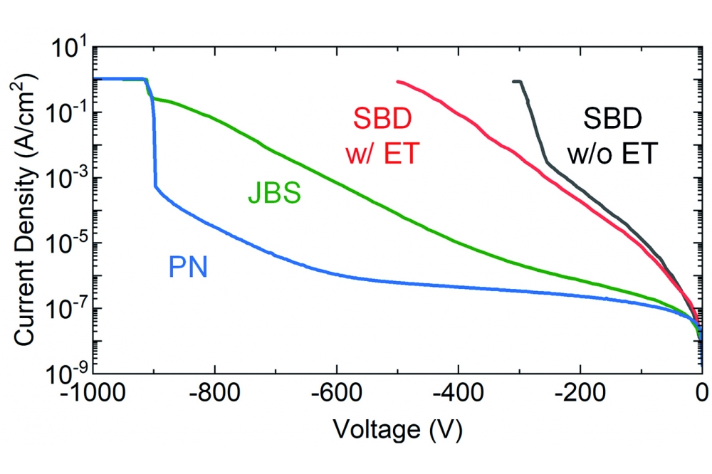
Electrical measurements of JBS diodes and Schottky diodes with edge termination revealed turn-on voltages of 0.75 V and 0.7 V, respectively, and an ideality factor of 1.03, indicating near-ideal Schottky behaviour. On-resistance for the JBS diode is just 0.6 mΩ cm2, a value that is claimed to be among the lowest for all GaN-based JBS devices. Reverse-bias measurements showed that the leakage current in the JBS diode is far lower than that for both forms of Schottky diode (see Figure). The breakdown voltage of the JBS diode is a record-breaking 915 V, according to the team.
According to Khachariya, the next targets are the development of larger diodes that are capable of handling 1 A to 100 A, and devices with a higher breakdown voltage capability of around 5 kV, realised by increasing the drift epilayer thickness and further reducing n-type doping.
Reference
D. Khachariya et al. Appl. Phys. Express 15 101004 (2022)


