
Laser lift off systems take off for microLEDs
3D-Micromac says more than ten microMIRA laser systems sold for microLED applications to date
3D-Micromac says more than ten microMIRA laser systems sold for microLED applications to date
3D-Micromac AG, a German maker of laser micromachining and roll-to-roll laser systems, has announced that a leading optical solutions provider has purchased multiple microMIRA Laser Lift-Off (LLO) systems from 3D-Micromac for use in the production of microLED devices.
The customer will install the new microMIRA systems in pilot- and production lines at its LED chip factory in Asia.
MicroLEDs have the potential to revolutionise the display industry, promising a variety of advantages such as superior viewing angle, high dynamic range with perfect black luminance and high brightness, wide colour gamut, fast refresh rates, long lifetime, and low power consumption. Potential applications include very large displays for indoor and outdoor use, as well as high-resolution displays for augmented reality (AR) and virtual reality (VR) wearable devices.
However, the microLED fabrication process is vastly more complex than LCD and OLED manufacturing, and faces several technical challenges that must be overcome before microLEDs can be readily available in the mass market. Among these challenges is detaching and transferring the processed microLED chips from the donor or growth substrate (e.g., sapphire) to an intermediate substrate for subsequent testing without damaging the expensive growth substrate, allowing it to be repurposed for future use. The microMIRA system from 3D-Micromac precisely addresses this task with superior performance.
3D-Micromac’s microMIRA system provides highly uniform, force-free lift-off of different layers on large-area substrates at high processing speeds without the need for costly and polluting wet chemical processes. The unique line beam system is built on a highly customisable platform that can incorporate different laser sources, wavelengths and beam paths to meet each customer’s unique requirements. The system is capable of processing different substrate materials and sizes, and can achieve processing speeds (including handling) of up to 60 eight-inch wafers per hour.
According to Uwe Wagner, CEO of 3D-Micromac: “This multiple system order is a testament to our ability to provide innovative and enabling laser micromachining solutions for industrial applications serving both mature and emerging markets. It also represents an important milestone for 3D-Micromac as we continue to expand our product offerings and services into the display industry, addressing the production needs for exciting new display technologies, including microLEDs. To date, 3D-Micromac has sold more than 10 laser processing systems for microLED applications, including our industry-benchmark microMIRA laser-lift-off system as well as our recently introduced microCETI micromachining platform.”
The microMIRA LLO system has been used successfully in mass production by electronics manufacturers for years. In addition to GaN lift-off from glass and sapphire substrates in microLED display manufacturing, the microMIRA system can also be used for layer separation in semiconductor and sensor manufacturing, as well as for laser annealing and crystallisation for surface modification.
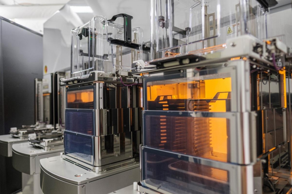
Pictured above is the load port for wafer cassettes for the microMIRA laser system. The system is capable of processing different substrate materials and sizes, and can achieve processing speeds (including handling) of up to 60 eight-inch wafers per hour.


