
Diamfab unveils dual business strategy
French diamond wafer start-up to sell technology directly and through application-oriented partnerships
Diamfab, a France-based start-up innovator of diamond semiconductor wafer technology for next-generation electronics, will move to a new dual business model strategy. Under this new approach, Diamfab will sell its technology directly and through application-oriented strategic partnerships and alliances.
Applications range from electric vehicles with diamond power electronics devices to IoT with 20 years long life battery, to nuclear and spatial applications with hardened electronics components or detectors in healthcare, and even ultraprecise quantum sensors for autonomous vehicles.
The plan is to achieve a scalable go-to-market model implemented through a mix of in-house capabilities and an extended partner ecosystem based on co-development. “Over the past two years, we have made significant progress working with R&D teams to process high value-added diamond wafers. Our application-oriented approach based on a dual business model will now allow us to work with a broader set of industrial partners, to develop and sell high value-added diamond wafers and our patented diamond devices manufacturing processes, while also selling directly to end users with a fab-light model,” said Gauthier Chicot, CEO of Diamfab.
Diamfab has already started to work with partners on the design and fabrication of high-performance devices including diodes, transistors, capacitors, quantum sensors, and high-energy detectors. The company’s first market is capacitors for electrical vehicles, where the advantages of diamond semiconductors over actual capacitor technologies show tremendous potential for improving compactness and performance over the lifetime of a vehicle.
“We have already filed a patent on an all-diamond capacitor and are collaborating with a leading player in this field,” said Chicot. Among other parameters, we have achieved our targets: a high current density of over 1000A/cm2 and a breakdown electric field larger than 7.7MV/cm. These are key parameters for the performances of future devices and are already superior to what existing materials like SiC can provide for power electronics. Moreover, we have a clear roadmap to reach 4-inch wafers by 2025 as a key enabler for mass production.”
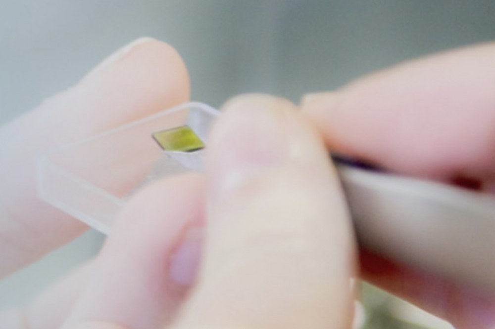
Diamond as a semiconductor
Diamond has 5000 times higher current density and 30 times higher voltage compared to silicon and can operate in harsh environments (high temperature and radiation). Diamfab’s patented approach to growing synthetic diamond material ranging from a few nanometers in thickness to tens of micrometers is thought to be unique in the industry.
Diamfab diamond wafers can be used for insulator, semiconductor, metallic, and superconductive conduction applications. In automotive applications, Diamfab wafers could allow the fabrication of 80 percent lighter and more compact power converters, according to the company. In power grid applications, Diamfab wafers could also more easily handle higher voltage and reduce energy losses by a factor of 10 compared to silicon.


