
3C-SiC enhances the GaN HEMT
GaN-on-silicon HEMTs with a 3C-SiC interlayer combine a relatively low transmission loss with a very high breakdown voltage
For the production of GaN HEMTs for power and RF applications, the silicon substrate has its pros and cons. It majors on a large, low-cost and widely available platform, but it is impaired by significant thermal and lattice mismatches with the epilayers – this gives rise to a high density of dislocations and cracking, imperfections that compromise the device’s performance, its reliability and its lifetime.
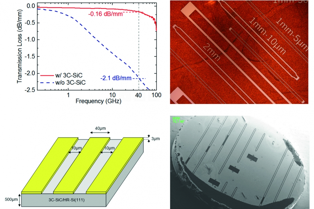
However, it appears that it’s now possible to enjoy the benefits of silicon, without having to suffer the weaknesses, by inserting a 3C SiC interlayer. Efforts by an international collaboration – led by researchers at the University of Sherbrooke, Canada, and supported by those at the Center for the Development of Advanced Technologies, Algiers; Liverpool John Moores University, UK; and the French institutions LIMMS/CNRS-IIS and IEMN/CNRS – have led to the fabrication of GaN HEMTs with a relatively low transmission loss of 0.16 dB/mm at 40 GHz, and a soft breakdown voltage of around 1530 V at 1 µA/mm, which is said to be three times larger than that of conventional devices.
The foundation for this work is an engineered substrate produced by Air Water Corporation that combines 500 µm-thick, high-resistivity (111) silicon with a 3C-SiC transition layer. Air Water Corporation has been working on 3C-SiC since the 1970s, and in 1992 it filed it first patent on GaN on 3C-SiC.
“It seems that this company has great experience in co-doping 3C-SiC, and has achieved high-quality crystal structures and high electrical resistivity,” remarked Brahim Benbakhti, who spoke to Compound Semiconductor on behalf of the collaboration, and is affiliated to both the University and Sherbrooke and the Center for the Development of Advanced Technologies.
Benbakhti and co-workers have investigated the growth of GaN-based structures on 3C-SiC-on-silicon, and also on just silicon, to provide a control – and they have fabricated and tested a range of devices produced from both these epiwafers.
Buffers for the devices were either a 3 µm-thick layer of AlGaN, employed for the control, or a 1.3 µm-thick layer of AlGaN deposited on a 1.7 µm-thick layer of vanadium-doped 3C-SiC. On both buffers the team added a 1.8 µm-thick Al0.18Ga0.82N back barrier, a 150 nm-thick undoped GaN channel, and a 4 nm-thick Al0.45Ga0.55N back barrier. In-situ growth of a 20 nm-thick SiN cap layer passivated the surface and prevented strain relaxation.
MOS HEMTs were fabricated with a source-to-gate spacing of 2 µm, a gate length of 1.5 µm, and a gate-to-drain distance of 15 µm. Measurements using coplanar waveguides, with dimensions optimised for 50 ohms impedance, revealed that inserting the 3C-SiC interlayer slashed transmission loss at 40 GHz from 2.1 dB/mm to just 0.16 dB/mm. This result is said to be superior to those obtained on substrates made from either GaN, high-resistivity silicon or diamond.
The researchers have also investigated the breakdown voltages of their transistors. The device with the conventional design exhibited an increase in leakage current beyond 300 V, with leakage hitting 1 µA/mm at 395 V. In comparison, the variant with the 3C-SiC interlayer required a drain-source voltage in excess of 1.5 kV to hit this value.
Benbakhti told Compound Semiconductor that reliability is the biggest obstacle to large-scale commercialisation of GaN-based devices with the 3C-SiC interlayers. “Therefore, the behaviour of the device and its lifetime, under different electrical and thermal stresses, needs to be investigated.
To date, GaN HEMTs with a 3C-SiC interlayer have been shown to be good candidates for power switching. “For RF power electronics, it is crucial to examine the thermal resistance introduced by the 3C-SiC interlayer, which could act as a thermal barrier and limit the device performance in RF,” commented Benbakhti.
Reference
A. E-H. Khediri et al. Appl. Phys Lett. 121 122103 (2022)


