
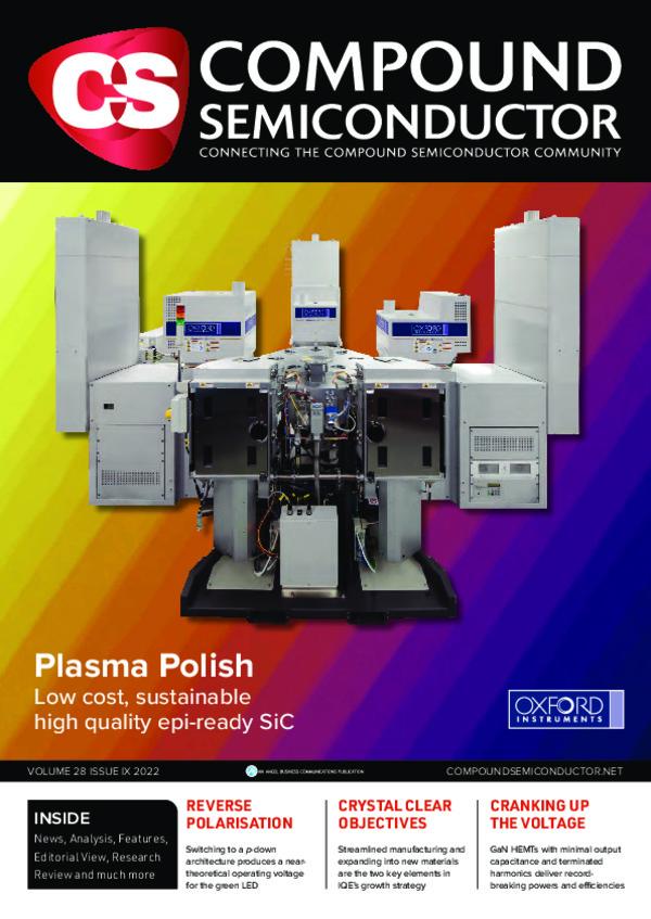
Plasma Polish enables SiC revolution
New lower-cost specialist SiC polish technique provides epi-ready surface, without compromising quality.
BY GRANT BALDWIN FROM OXFORD INSTRUMENTS PLASMA TECHNOLOGY
Elon Musk is not a paint-by-numbers operator. Instead, he’s leading the commercial space race, he’s playing the crypto currency game like a grandmaster, and he’s just closed a Twitter purchase deal that’s been a white-knuckle ride for investors and representatives of the microblogging social network site.
Musk is as interesting as he is shrewd. He has a propensity for pushing boundaries, exemplified by his automotive jewel Tesla, pioneer of the electric vehicle (EV) market, and the first adopter of SiC inverters. At the heart of every EV is a drive train inverter, normally operating at 400 V, that converts DC battery output into an AC form that propels the vehicle. SiC had an early adopter in Tesla, bringing it recognition as the material of choice for this class of application. This has spawned broader adoption and ramping demand for this advanced compound material – also making it commercially attractive at today’s device price point.
Cost aside, the automotive industry is a conservative market that does not move quickly. Reliability must be proven, so rushing innovation is imprudent, considering the preciousness of the cargo. However, the importance of SiC components in E-mobility, as well as in other sectors, such as solar and industrial markets, is prompting the makers of these wide bandgap devices to develop enticing new technologies and processes to meet the performance, reliability and volume demands of these markets.

Etch, deposition and thermal growth module options
There are still some high-end vehicles that utilise the alternative silicon IGBT, but the number of models adopting this form of transistor is vanishingly small and diminishing rapidly. At 400 V operation SiC is very proficient, but will not dominate there because silicon is still quite strong in that space. At 800 V operation using 1200 V rated devices, SiC demonstrates far faster switching speeds than the silicon IGBT – leading to lighter, more efficient and smaller inverters, with fewer cooling requirements. Drawing on all these strengths is key to trimming the battery size required to extend the target range on a single charge. These advantages, already apparent at 400 V, are magnified at 800 V, strengthening the argument for SiC over silicon.
SiC versus silicon
Like silicon, SiC can be grown in boules. They are sliced into substrates ready for epitaxial growth and device fabrication. The SiC industry is currently ramping production of diodes and MOSFETs, and in time this portfolio could be extended to include IGBTs and thyristors.
Due to the comparable nature of SiC and silicon, their devices bear striking similarities. However, SiC offers higher performance, and there are also cost variations when comparing at both the unit and the system level. One key difference is the cost associated with wafer fabrication – this is far higher for SiC, because it’s an incredibly hard material. There are also some SiC-specific techniques, such as the gate fabrication process, required to get channel mobility as high as possible, and the final wafering step prior to epi. For the latter there’s now a new process from Oxford Instruments called Plasma Polish – more on that below.
By far the biggest cost is energy. It is incurred right from the start and is embedded in the wafer from very early in the wafering process. Silicon can be grown cheaply and easily, because this process requires a modest amount of energy, compared with SiC, to liquify the silicon and make boules. Silicon boules, cylindrical crystals that are sliced into wafers, can have diameters of more than 300 mm and a length of more than a meter.
In stark contrast, bulk SiC is produced via a seeded sublimation process, which is very slow compared to silicon, taking up to a week to produce a 150 mm diameter boule – although 200 mm is on the way. Production is incredibly energy intensive, with the high costs embedded in the bouling process carried through to device costs.
The cost benefit of shifting SiC production from 150 mm to 200 mm wafers is based on the principle that the larger diameter allows more devices, making each wafer more valuable. However, it’s important to note that the energy cost increases proportionally with the wafer surface area, so while 200 mm SiC is certainly essential to advance its wider adoption, when trying to reduce cost per device for SiC, it’s no magic bullet.

Yield data highlights that the Plasma Polish process developed by Oxford
Instruments delivers a device yield of SiC merged p-i-n diodes that is
at least as high as that resulting from CMP.
What’s slowing adoption?
The strongest headwinds to the deployment of more SiC devices tend to be associated with costs, but there is also additional effort required to make the switch from silicon to SiC for OEMs. Reliability, robustness, efficiency and performance are all cost drivers that really matter to the automotive industry. Every maker of EVs has a SiC development programme, as this material is widely regarded as key to the rollout of this class of automobile. A key consideration from consumers driving the switch to SiC is increased range on a single charge, while looming political deadlines, such as California’s internal combustion engine ban that’s expected in 2035, is accelerating mass EV adoption.
The current silicon solution is cheap, its properties and engineering limitations are well understood, and despite automotive OEMs being one of just a handful of industries with deep enough pockets to fund this type of development, new devices need to be robust and price competitive. However, as 800 V inverters expand from the likes of the Porsche Taycan and the Audi e-tron GT to the majority of EVs, SiC will start to become the more obvious choice over the silicon IGBT. Once mainstream vehicles start to pack SiC technology, the tide will have turned for sure for SiC over silicon.
Power generation cost per unit in some circumstances can be as much as five times higher for SiC compared with silicon. Shifting to 200 mm and benefiting from the associated economies of scale should enable the price to come down, but further progress will require a reduction in both substrate fabrication cost and epi cost, as they are the two most expensive processes after the boule is formed. The key point is that a move to 200 mm wafers may not be the panacea some believe it to be. It’s all about energy, and this energy cost is embedded into the 200 mm boule. Consequently, when taking all factors into consideration, if SiC devices are to achieve cost parity with silicon, 200 mm wafer capability will have to go hand-in-hand with SiC-specific advanced substrate fabrication techniques and solutions.

The AFM by Oxford Instruments Asylum Research offers an insight into
surface morphology. This tool provided an image of the surface of a SiC
wafer, used on the background of the front cover of this magazine.
Advancing fabrication
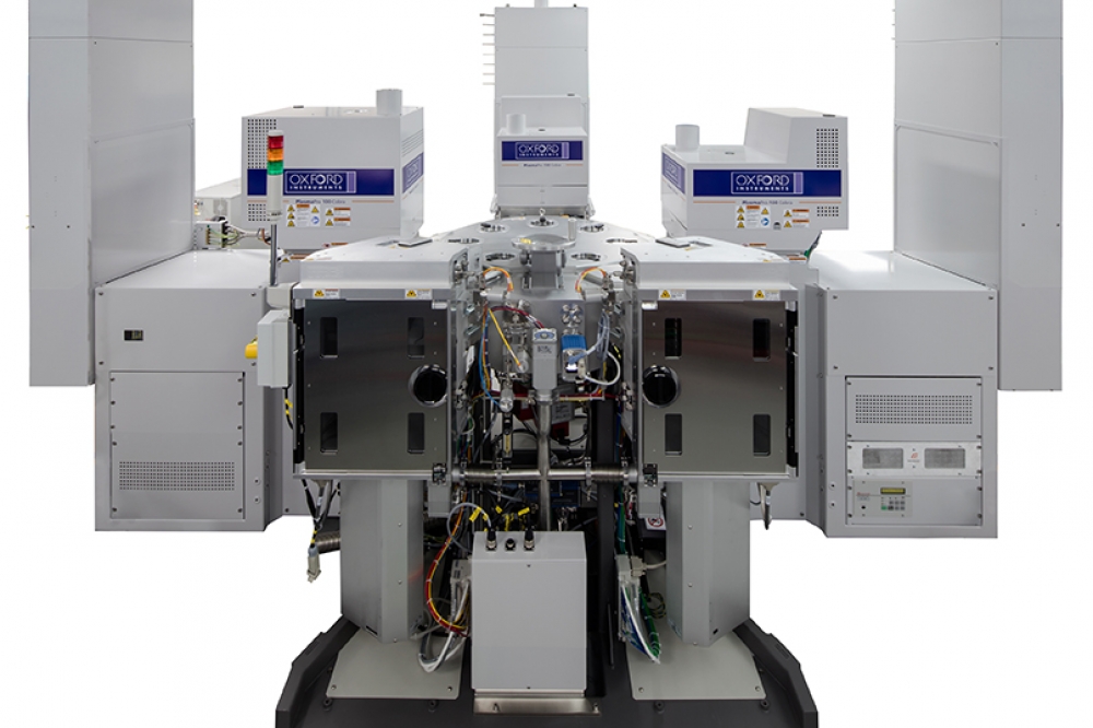
At this year’s International Conference on Silicon Carbide and Related Materials (ICSCRM), held in September in Davos, Switzerland, our team at Oxford Instruments Plasma Technology launched a Plasma Polish process for SiC substrates. Our new process is cleaner, greener and more cost-effective than the incumbent, chemical mechanical polishing (CMP). Plasma Polish can be implemented as a direct plug and play replacement for CMP, fitting neatly into the space where CMP currently sits.
There are three key steps in the process for creating substrates ready for epitaxial growth and subsequent device fabrication. Those critical steps are: boule growth; slice and grind; and then polish. The purpose of the polish is to reduce the SiC surface roughness to a point where it is sufficiently smooth for epitaxial growth.
CMP achieves epi-ready smoothness by applying rotating abrasive discs to the surface of the substrates with pressure. This is accompanied by proprietary, expensive slurries, which chemically treat the surface. To prevent clogging during this process, flushing removes material from the discs. CMP is well-established, having been used for many years to achieve epi-ready smoothness, but it suffers from some limitations that are overcome with Plasma Polish.

Plasma Polish penetrates into the sub-surface, repairing damage.
One substantial limitation is the use of slurry, an expensive component to acquire and dispose of afterwards, as it is a semi-toxic by-product. Additional costs arise due to the need for lots of water – as much as 40 percent of water usage throughout the semiconductor fabrication industry is associated with CMP. Lastly, there is the requirement to regularly replace the abrasive discs, which adds cost and supply chain complexity.
Another issue is the suitability of CMP in relation to yield for SiC devices. While CMP has undoubtedly been a great success for processing silicon, is it the ideal process technique for harder semiconductor materials? As SiC is one of the hardest materials used in any industry, it requires more mechanical pressure during the polish step than silicon. At surface level, CMP has a positive effect on improving material quality ready for epitaxy, but the additional polishing force required to improve the top surface can negatively impact the sub-surface. Too much mechanical pressure and friction-generated heat can cause micro fissures to form in the subsurface, which are not ideal for material quality and can cause lower device yield.
Our approach offers an attractive alternative that can accelerate SiC adoption by combining high-quality results with a reduction in cost. It is a dry-etch process, taking place in a chamber held at a low pumping pressure. A chemically reactive plasma is accelerated onto the wafer surface with electromagnetic force, leading to chemical and physical removal of the material. There’s no need for slurry or water (other than recirculated cooling water), and thanks to the absence of moving or wearing parts, consumable costs are minimal compared to CMP.
As it is contactless, no physical pressure is applied to the wafer during Plasma Polish, so sub-surface damage is actually improved. The gas in the Plasma Polish process also has a lower density than the slurry used in CMP; and it is electromagnetically accelerated onto the wafer surface, rather than squirted on, as is the case for a slurry with CMP. These key differences enable the Plasma Polish process to penetrate deeper into the damage left behind by the slice/grind wafering step. The plasma physically knocks off and chemically attaches to the weakly bonded and damaged SiC surface and sub-surface. The material that remains is more strongly bonded and therefore higher quality, making it preferable for higher-yielding devices.
Our SiC Plasma Polish tool, which is suitable for processing 200 mm wafers, has been configured to 150 mm during process development. Plasma Polish is a great addition to our established portfolio of production tools for 200 mm wafers.
Over the years, we have transferred many processes to larger sizes, as wafer diameters have increased. We understand the process transfer well, but it’s just a lack of commercially available 200 mm SiC substrates that is preventing Plasma Polish at 200 mm.
Too good to be true?
When we announced our Plasma Polish technology at the recent ICSCRM, a few delegates wondered if it sounded a bit too good to be true. A little bit of scepticism is certainly healthy, but we would argue that our solution falls into the category of ‘why didn’t someone think of it sooner?’
Rather than debating pros and cons, we simply share our validation data, which speaks louder than words. This data comes from an investigation carried out in partnership with the Scottish specialist SiC wafer foundry Clas-SiC Wafer Fab, where we ran Plasma Polished and CMP-treated wafers side-by-side to device production.
The performance of merged pin diodes and 1200 V MOSFETs is comparable, or arguably slightly better for the Plasma Polish process. This led David Clark, Technology & Customer Relations Manager at Clas-SiC, to comment that Plasma Polish is a very important technology for reducing the cost of SiC-based power converters and increasing their adoption.
We have also identified further uses for the Plasma Polish process. It can be utilized by SiC boule manufacturers, to prepare the underside of the SiC seed wafer in preparation for the sublimation process.
Currently that wafer surface is processed using CMP, so there are opportunities for cost savings and improvement to material quality there. In addition, Plasma Polish could be applied to semi-insulating undoped SiC substrates used for RF applications, as well as several other applications that our developers are keeping under wraps for now.
The rubber meets the road
A single technological advance will not be enough to bring SiC to mainstream adoption. What’s needed is to stack several marginal gains to reach the tipping point for this advanced material. It’s essential to think beyond the silicon processing techniques that worked well for that material, because SiC has fundamentally different properties and performance.
We are now a step nearer. We are on the cusp of 200 mm capability, along with a new technology for wafer polishing that’s cleaner, greener and cost-competitive. Once this is combined with other SiC-specific processing techniques, the foundations will fall into place for an E-mobility and sustainable energy revolution.
Ballroom and through-wall cassette load configurations are available


