
A game changer: Epitaxially grown nitride ferroelectrics
Precisely tuning electrical polarization switching of nitride
semiconductors provides a pivotal step towards next-generation
electronics.
BY PING WANG, DING WANG AND ZETIAN MI FROM THE UNIVERSITY OF MICHIGAN
Ferroelectrics have a big part to play in tomorrow’s world. They are critical to the development of next-generation electronic, optoelectronic, acoustic and quantum devices. The desired characteristics are a high Curie temperature, a large electromechanical response, a large remnant polarization, a wide range tuneable operating voltage, a high crystalline quality and a compatibility with mainstream semiconductor technology. Ferroelectric materials with all those attributes can produce transistors, memristors, sensors, actuators, quantum switches and transducers operating at high powers, high frequencies, high efficiencies and high-speed, while drawing very little power.
Over the last few decades there has been significant advancement in the theoretical models, material synthesis and characterization of ferroelectrics. A key milestone came in 2011, with the discovery of ferroelectricity in doped HfO2. Since then, ferroelectrics have been taken more seriously, and have been integrated into some mainstream semiconductor manufacturing processes. However, the commercialization of HfO2-based devices has been held back by challenges associated with ferroelectric phase stability, an imprint issue, the wake-up effect and a high coercive field.
One promising class of piezoelectric material that is well known to all of us is AlN-based nitride semiconductors. They exhibit a strong spontaneous polarization along the c-axis, leading to two stable lattice states – metal-polar and nitrogen (N)-polar – with opposite polarization. In principle, these two states are electrically switchable via an intermediate metastable hexagonal phase. Unfortunately, due to the giant energy barrier between the wurtzite and hexagonal phases, this transition cannot happen without causing dielectric breakdown.
Despite this drawback, the spark of interest has not been extinguished. Twenty years ago, working independently, researchers in the US and Mexico predicted the existence of wurtzite-phase, scandium-based III-nitrides (Sc-III-N) with a distorted lattice. These calculations indicate that there is a chance to reduce the polarization switching energy barrier. Detailed theoretical studies have strengthened the case, but there is yet to be much experimental progress.
Realising ferroelectricity in nitride semiconductors is expected to unleash a significant revolution on the research of not only third-generation wide bandgap semiconductors, such as GaN, SiC and AlN, but also on ferroelectric materials in general. Spurred on by the abnormal enhancement of the piezoelectric response observed in ScAlN alloys by a team from the National Institute of Advanced Industrial Science and Technology, Japan, in 2009, much effort has been directed at exploring this alloy as the first candidate for providing ferroelectricity in nitride semiconductors.
In 2019 a German collaboration between the University of Kiel and the Fraunhofer Institute for Silicon Technology reported significant progress in ScAlN ferroelectrics. This partnership demonstrated ferroelectric polarization switching in sputtered polycrystalline ScAlN films, which possess a remnant polarization in excess of 100 µC cm-2 and a paraelectric transition temperature in excess of 600 °C.
Motivated by this success, funding programmes emerged almost immediately in several countries to support further research. From that point on, it’s been a race to see who could grow this class of ferroelectric semiconductors with a process that’s compatible with mainstream semiconductor technologies.
A fundamental building block to fulfilling this goal is the epitaxial growth of nitride ferroelectrics. MOCVD and MBE are obvious options, given their success in high-throughput growth of many III-nitride device structures, such as LEDs, laser diodes and HEMTs. However, the growth of Sc-III-N by either MOCVD or MBE is extremely challenging. Efforts have been underway since the turn of the millennium, with early studies tending to focus on the addition of scandium into GaN, due to the tuneable bandgap of ScGaN in the visible domain. Highlights include a report from Ohio University of wurtzite-like growth of a ScGaN alloy by MBE in 2004, and the finding by a team from Sandia National Laboratories of the incorporation of scandium in GaN at the doping level, realised by MOCVD and announced in 2009.
Due to a complicated phase diagram, epitaxial growth of crystalline ScAlN is more elusive than its ScGaN cousin. This challenge explains why the experimental growth of the later has only recently been reported. Initial success came from a team from the Naval Research Laboratory, reporting MBE growth of wurtzite phase ScAlN films in 2017. A German collaboration between the Fraunhofer Institute for Applied Solid State Physics IAF and INATECH – Albert-Ludwigs University Freiburg has claimed similar success, using an upgraded MOCVD system.
While these milestones are important, they did not ensure the demonstration of ferroelectricity in ScAlN. For that crucial breakthrough, success has recently come from our team at the University of Michigan. To succeed in that endeavour, we had to increase the breakdown field beyond the polarization switching field – that is, the coercive field. This move is critical to overcoming the switching energy barrier between metal-polar and N-polar lattice states.
For this work we selected MBE. It is an excellent technique for epitaxy of nitride semiconductors in an ultra-high vacuum environment, thanks to its high controllability of impurities, doping levels, interfaces, domain structure, lattice-polarity and so on. Crucially, it can enable full integration of nitride ferroelectrics with workhorse GaN and silicon technologies, as well as thickness scaling down to a single atomic layer.
The significant advantages of MBE over other epitaxial techniques has led our team to conduct several systematic investigations that span material growth to the demonstration of ferroelectricity and the development of a broad range of devices. Over the years we have accumulated rich experience surrounding the control of phase purity, crystal quality, impurity incorporation, interface quality and lattice-polarity. This expertise has provided a great foundation for realizing ferroelectricity in epitaxial, single-crystalline ScAlN films.
High-quality material is at the heart of fundamental material studies and practical device applications. Thanks to the tremendous freedom offered by a versatile MBE system, we can readily explore and optimize conditions for depositing single-crystalline, wurtzite-phase ScAlN with high crystal quality, atomically sharp interfaces, a high breakdown field and a controllable scandium content (see Figure 1 (a)).

Figure 1. (a) Diagram and scanning tunnelling electron microscopy image
of the ScAlN/GaN interface. Taken from D. Wang et al. Adv. Electron.
Mater. 8 2200005 (2022). (b) Polarization-electric-field loops measured
at 40 kHz for ferroelectric ScAlN with varying scandium content. (c)
Remnant polarization during the endurance test for Sc0.20Al0.80N using
10 μs pulse width. Taken from P. Wang et al. Appl. Phys. Lett. 118
223504 (2021)
We have passed many milestones on our road to realising epitaxially grown ferroelectric ScAlN and related devices. To establish the possibility of integration and maximize the potential applications for ferroelectric ScAlN with GaN architectures, we have focused primarily on ferroelectricity in polar ScAlN/GaN heterostructures.
MBE-grown ferroelectric ScAlN
When we increased the breakdown field in our MBE-grown ScAlN films beyond the electric field that is needed for polarization switching, we observed the first ever clear box-like hysteresis polarization over electric field loops. This finding, seen in ScAlN films with various scandium compositions (see Figure 1 (b)), offers strong evidence for ferroelectricity. Strengthening the case are detailed electrical measurements and piezoresponse force microscopy studies.
If ferroelectric ScAlN is to serve in practical device applications, it must be stable and reliable. Initial results have been very encouraging, with electrical poling in our MBE-grown ScAlN films presenting a polarization retention time beyond 105 s, with negligible degradation in 10 years. Our endurance tests uncover no obvious fatigue, with up to 105 times bipolar electrical cycling (see Figure 1 (c)).
Recently, we have obtained even more impressive results, including an increase in the endurance strength beyond 107 cycles. With further studies and optimization, we are confident that reliability during electrical cycling for ScAlN will surpass that of the commonly studied HZO and PZT ferroelectrics.
As part of this investigation, we have demonstrated fully epitaxial ferroelectric ScAlN/GaN heterostructure memristors. These devices show stable operation at a high temperature of 670 K, which is close to or even above the Curie temperature of most conventional ferroelectrics.
MBE-grown ferroelectric ScGaN
Polarization is what makes III-nitrides unique. This opportunity to control and switch the polarization opens up new applications in memory, reconfigurable power devices and piezo devices, as well as quantum photonic devices with unprecedented stability, performance and functionality.
With this goal in mind, we have turned our attention to a related but less explored class of material, ScGaN, which has been shown to have a level of ferroelectricity similar to ScAlN. However, prior to our work there has been an absence of experimental demonstration of ferroelectric ScGaN, produced by either sputtering or epitaxial growth.
We have formed wurtzite ScGaN films on GaN by MBE, using similar growth strategies that we used to produce epitaxial ScAlN. By carefully adjusting the scandium composition we have discovered a narrow window where ferroelectric ScGaN is accomplished and lattice-polarity electrically switched (see Figure 2). Following our study, researchers from the National Institute of Advanced Industrial Science and Technology in Japan have also reported ferroelectricity in sputtered ScGaN films.
Given the widely tunable bandgap between AlN and GaN, realising ferroelectricity in fully epitaxial ScAlN and ScGaN promises to provide a unique material platform with an unprecedentedly tuneable lattice, bandgap, polarization, and ferroelectricity.

Figure 2. (a) Loops of current density as a function of electric field
at 10 kHz for ScGaN films with varying scandium content. (b) Loops of
polarisation as a function of electric field, extracted from a set of
unipolar triangular waveform sequences with a frequency of 10 kHz. Taken
from D. Wang et al. Appl. Phys. Lett. 119 111902 (2021).
N-polar ferroelectric ScAlN
One of the most promising applications for ScAlN is as the barrier layer in a GaN-based HEMT. Analogous to AlGaN and InAlN, ScAlN, because of its significant spontaneous polarization, promises to increase the operating frequency at high power. Impressive results on metal-polar ScAlN/GaN HEMTs were reported back in 2019 by a collaboration between researchers at the U.S. Air Force Research Laboratory and Qorvo.
The alternative to this, the N-polar GaN-based HEMT, has intrinsic advantages. It allows increases in operating frequency while maintaining high output power and addressing scaling challenges. We have pursued this particular design, and by controlling the lattice-polarity of the underlying GaN buffer, we have used MBE to demonstrate the first N-polar ScAlN HEMT structures on an on-axis sapphire substrate. We measured a Hall mobility of 564 cm2 V-1 s-1, a sheet electron concentration of 4.1 x 1013 cm-2, and a sheet resistance as low as 271 Ω/sq.
Recently, we made further progress, demonstrating ferroelectricity in N-polar ScAlN/GaN heterostructures. These nearly lattice-matched heterostructures exhibit a highly uniform coercive field of around 4.6 MV/cm at 10 kHz, and a remnant polarization of around 90 µC cm-2 across the whole wafer (see Figure 3).
Our promising results could be surpassed with even more impressive ones by improving material quality and suppressing leakage. We are keen to explore electrical leakage paths in ferroelectric Sc-III-N films, as this will lay the foundation for establishing a robust growth strategy for addressing the leakage issue. Additionally, we will perform systematic microscopy studies to understand the polarization switching dynamics and the fatigue mechanism at scales from the micro to the atomic scale, enabling us to realise reliable ferroelectricity in fully epitaxial Sc-III-N heterostructures.
Another goal of ours is to develop nitride-ferroelectric-based electronic, optoelectronic and quantum devices and systems that are CMOS compatible and capable of combining high frequencies with high powers, a high efficiency and a low power consumption. Such devices could be deployed in automobile/aircraft/turbine engines, smart/electrical vehicles, 5G/6G communication technologies, big data analysis, the Internet of Things, and quantum sensing and communication. As an emerging member of third-generation semiconductors, as well as the ferroelectrics family, Sc-III-N exhibits great potential to be a unicorn in all these applications. In our recent works, we have also reported exciting results on photovoltaic detectors, memristors, transistors, and acoustic resonators.

Figure 3. (a) Scanning electron microscopy (SEM) images of as-grown
(left panel) and wet chemical etched (10 wt. TMAH at 50 °C for 5 min,
right panel) surface morphology for an N-polar ScAlN epilayer (upper
panel) and a GaN buffer (lower panel). All SEM images share the same
scale bar. (b) Coercive field and remnant polarization measured in 10
randomly distributed ferroelectric N-polar ScAlN/GaN capacitors. Taken
from P. Wang et al. Appl. Phys. Lett. 121 023501 (2022).
Bright prospects for nitride ferroelectrics
From a fundamental material discovery perspective, the recent demonstration of nitride ferroelectric semiconductors has showcased the feasibility of developing a portfolio of new ferroelectrics by incorporating in III-nitride semiconductors a range of rare-earth elements, such as yttrium, lanthanum and lutetium; another potential addition is boron. This avenue offers unprecedentedly rich opportunities for strain, alloy, quantum and entropy engineering.
For device development, an intuitive approach is to combine nitride ferroelectrics with state-of-the-art III-nitride devices, such as HEMTs, LEDs, laser diodes, photodetectors, waveguides and resonators. This move could enhance device performance and tunability, and add programmability, data storage and computing capabilities.

Sc-III-N research at the University of Michigan. From left to right:
Dr. Ding Wang, Dr. Ping Wang, and Prof. Zetian Mi. (Photo by Brenda
Ahearn)
One recent experimental breakthrough has been the overcoming of Boltzmann’s Tyranny by using the negative capacitance in ferroelectric materials. This advance highlights that nitride ferroelectrics will provide new opportunities for developing low-power-consumption transistors.
Ten years ago, the discovery of ferroelectricity in hafnium-based materials renewed interest in ferroelectrics. Now, this topic has been revitalised again, with the discovery of nitride ferroelectrics fuelling a new wave of research on ferroelectric semiconductor devices.
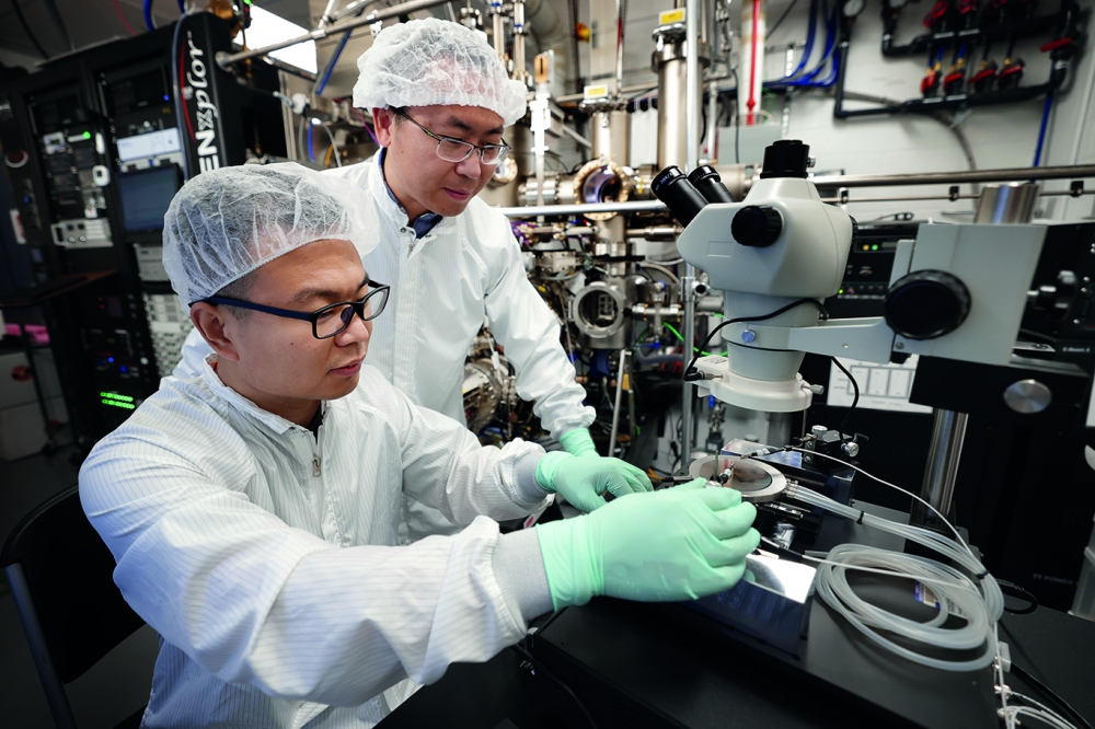
Main image: Left: Ferroelectricity testing of MBE-grown ScAlN films. (Photo by Brenda Ahearn)
Further reading
† P. Wang et al. Appl. Phys. Lett. 116 151903 (2020)
† P. Wang et al. Appl. Phys. Lett. 118 223504 (2021)
† D. Wang et al. Appl. Phys. Lett. 119 111902 (2021)
† P. Wang et al. Appl. Phys. Lett. 119 082101 (2021)
† D. Wang et al. Adv. Electron. Mater. 8 2200005 (2022)
† P. Wang et al. Appl. Phys. Lett. 121 023501 (2022)
† D. Wang et al. Appl. Phys. Lett. 121 042108 (2022)


