
NIST and AIM team up on photonics chips
Collaborative effort will enable new chip designs for high-speed communications
The US Department of Commerce’s National Institute of Standards and Technology (NIST) has entered into a cooperative research and development agreement with AIM Photonics that will give chip developers a critical new tool for designing faster integrated photonic circuits for use in high speed communications.
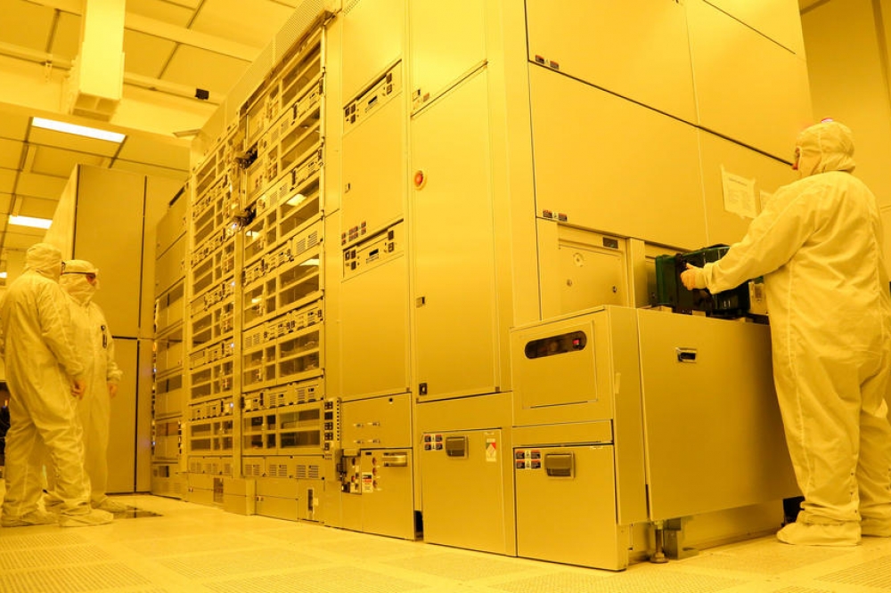
AIM Photonics, a Manufacturing USA institute, is a public-private partnership that accelerates the commercialization of new technologies for manufacturing photonic chips. The New York-based institute provides small and medium-sized businesses and academic and government researchers access to expertise and fabrication facilities during all phases of the photonics development cycle, from design to fabrication and packaging.
As part of the new collaboration, NIST will design electrical “calibration structures” that can be used to measure and test the electronic performance of the chips. This will result in improved designs for photonic chips that operate at speeds up to 110 gigahertz (GHz). Most current photonic chips operate at around 25 GHz.
“This effort will leverage NIST’s expertise in chip measurements, calibration and integrated device modeling,” said Under Secretary of Commerce for Standards and Technology and NIST Director Laurie E. Locascio. And while planning for this effort began before the passage of the CHIPS Act, it aligns with the act’s goals. “This shows how government and industry can work together to drive innovation and restore U.S. global leadership in semiconductor manufacturing,” Locascio said.
In addition, AIM Photonics will incorporate these calibration structures into its process design kit, a tool that engineers use when designing new chips for fabrication at AIM’s facilities.
“Accurate measurements are key to advancing high-speed communications,” said David Harame, AIM Photonics’ chief operating officer. “These enhancements will give our members and customers the tools they need to design the next generation of advanced photonic chips.”
Experts from both organisations are already working to integrate the new measurement structures into AIM Photonics’ foundry process, and an updated process design kit with the calibration structures should be available to users in approximately one year.


