First monolithic micro-LED display using organic TFTs

SmartKem uses semiconductor inks to process transistors directly on top of GaN LEDs
SmartKem, a company based in Manchester UK, has announced the world’s first monolithic micro-LED display using organic thin-film transistors (OTFTs). It says this new method of processing a thin-film transistor backplane on top of GaN LEDs has the potential to accelerate the commercialisation of micro-LED displays.
Consumer electronics companies are developing micro-LED displays since they promise higher brightness, lower power consumption and longer lifetime. This is particularly important for portable powered displays such as smartwatches and AR/VR displays which cannot accommodate large batteries.
Today’s existing VR & AR headsets use LCD and OLED displays, lacking brightness, resolution, power efficiency and lifetime. Existing efforts at establishing micro-LED manufacturing use physical transfer of LEDs from the wafer upon which they are manufactured to the TFT display backplane, where they must be laser welded to the contact pad of the transistor to make an electrical connection.
Since, for high resolution displays, millions of tiny LEDs need to be transferred from one place to another, then the potential for placement error is large. If a 99.9 percent placement yield is achieved, then a full HD colour display will have over 6,000 faulty sub-pixel LEDs that would need to be identified, removed, and re-attached. Once the 6,000 faulty LEDs have been replaced, a 99.9 percent yield will still mean six of these will be faulty, so your job of manufacturing a perfect display is not yet finished. It is the process of seeking out the faults and then replacing them one by one which is slowing down commercialisation of this new type of display.
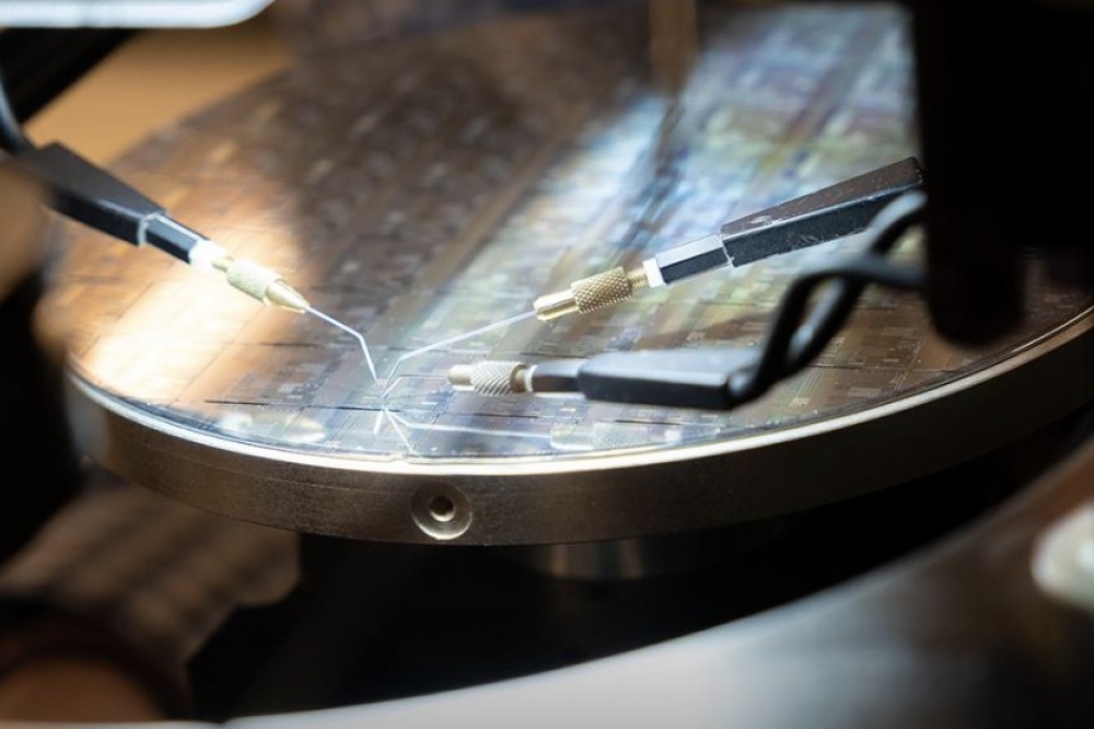
SmartKem’s patented core chemistry allows its semiconductor inks to be processed at the low temperature of 80°C. With this lower temperature, you can process its transistors directly on top of the micro-LEDs. This eliminates the mass transfer and laser welding processes, and the fabrication of OTFTs can use existing low-cost manufacturing tools currently used for LCD backplane manufacturing.
This approach cannot be carried out with other types of thin-film transistors as they are processed at the much higher temperature of 300°C, which damages the micro-LEDs, and is why you need to make them separately and then laboriously join them together one by one.


