
Red microLEDs: Brighter and better
Moving to arsenic-free AlInGaP-based heterostructures enhances the key characteristics of red microLEDs while retaining their compatibility with CMOS processing lines.
BY RICHARD STEVENSON, EDITOR, COMPOUND SEMICONDUCTOR
Interest in displays based on microLEDs is sky high. The tremendous capabilities of these miniature marvels – including exceptional efficiencies, a simple approach to scaling dimensions and incredibly long lifetimes – makes them very attractive candidates in many forms of display, from smartwatches and augmented-reality glasses through to TVs and video walls.
However, realising commercial success in all these types of display will not be easy. For the production of larger displays there has to be a picking and placing of millions and millions of tiny red, green and blue LEDs, a task that cannot be completed quick enough with today’s tools.
It is more likely that the first significant sales of displays deploying microLEDs will come from an uptake of augmented reality. For this type of application, arrays of single-colour LEDs formed on silicon wafers can be bonded to ‘backplane’ ICs that drives the pixels – with colour images constructed via optics that draws together the emission from red, green and blue arrays.
The challenge with this approach is to produce efficient emission in the red. It’s not possible to shrink the conventional red-emitting LEDs used for the likes of automobile brake lights to the micro-scale, because these established devices contain arsenic, which is outlawed in CMOS lines. And the obvious alternative, extending the emission of nitride-based devices that excel in the blue and green to the red, leads to plummeting efficiencies.
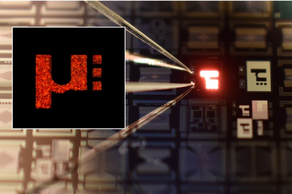
But there is a way to avoid both these pitfalls: make red microLEDs from an arsenic-free stack that’s based on AlInGaP and grown on silicon. That’s the trailblazing technology developed by imec spin-off Micledi, which unveiled its triumph at this year’s Consumer Electronics Show (CES), held in Las Vegas at the beginning of January. The devices produced in this manner are a more compelling alternative to the company’s more conventional, GaN-based red microLEDs, which emit broader emission at shorter wavelengths.
Micledi’s first AlInGaP microLEDs have an emission peak at 653 nm. That’s probably about 15-20 nm higher than needed, according to the company’s VP of Business Development, Harold Blomquist. However, he says that it’s nice to have the extra headroom.
As well as substantially stretching to longer wavelengths, Micledi’s AlInGaP microLEDs provide a far narrower spectral width, with a full-width at half-maximum below 9 nm, compared with less than 50 nm for nitride-based variants. This hike in spectral purity aids efforts to direct far more of the emitted light into the viewing angle, thanks to less dispersion.
The Belgium-based company decided to develop AlInGaP microLEDs because they reasoned that they may have more promise than their nitride siblings, which have shown slow progress, despite being studied by many groups for many years. Working with partners, Micledi’s recent success is the culmination of at least a year’s efforts.
Production of the company’s displays starts with the sourcing of epiwafers from various suppliers. “We are really agnostic to epi-materials, because good epi comes in 6-inch wafers, it comes in 8-inch wafers, and we want to use the best epi material,” argues Blomquist.
Epiwafers are chopped into display-sized chiplets, which are bonded to a 300 mm carrier wafer and dispatched to a semiconductor fab, where 300 mm lithography defines the dimensions of the microLED. This approach ensures very tight process control and excellent repeatability across the entirety of every wafer.
Not that long ago it was far from easy to secure a slot in a 300 mm fab, but times have changed markedly, says Blomquist. “We’re not bound by 18-to-24 month sold out manufacturing profiles. There is today a much more open-minded interest in looking at [processing our material] as a way to utilise older process nodes.”
The sector with the biggest promise right now, stylish glasses sporting microLED-enabled augmented reality, is still to emerge. But variants of this technology are starting to appear in industrial and enterprise sectors, through product launches from the likes of Vuzix and Magic Leap, both exhibitors at CES.
In industry, augmented-reality glasses are able to aid the capability of operators at work stations, offering guidelines, instructions, and providing images of what to do; and in medicine they can support surgeons, who are better-positioned to exchange ideas with other medical professionals located outside of the operating theatre.
While some will be sceptical whether AR glasses will ever catch on with consumers – there are those that will surely shy away from such an immersive experience – Blomquist is adamant that this technology will take off. He is convinced that AR glasses will become a must-have for younger generations, who will revel in reading their latest messages and following social media while their phones remain in their pockets.
Before this revolution takes place, there will have to be improvements to the brightness of displays, alongside a trimming of their operating power, size and weight.
Alongside these long-term goals, Micledi has another, based on the driving technology. The company currently uses a passive matrix, which provides a lot of flexibility, in terms of illumination, images and device characterisation. “But we are working very seriously on bringing out an ASIC backplane, to bring an active matrix solution into the marketplace just after the middle of the year.”
With progress on multiple fronts, Micledi is destined to be a key player in the growth of microLED displays

Red LED using AlInGaP: Switching from GaN to AlInGaP enables a shift to longer wavelengths and a reduction in the width of the emission peak.


