
Confined structure aids 2D material growth
Researchers say new growth technique allows them to build single domain layer-by-layer heterojunctions at the wafer-scale
An international team has reported on a new method to grow 2D transition metal dichalcogenides (TMD) for next-generation electronics. Their paper 'Non-epitaxial single-crystal 2D material growth by geometrical confinement' was published in Nature.
The team, co-led by Sang-Hoon Bae at the McKelvey School of Engineering at Washington University in St. Louis, Jeehwan Kim at MIT, and Jin-Hong Park at Sungkyunkwan University, had to overcome three challenges to create the new materials: securing single crystallinity at wafer-scale; preventing irregular thickness during growth at wafer-scale; and vertical heterostructures at wafer-scale.
Bae said 3D materials go through a process of roughening and smoothing to become an even-surfaced material. However, 2D materials don’t allow this process, resulting in an uneven surface that makes it difficult to have a large-scale, high-quality, uniform 2D material.
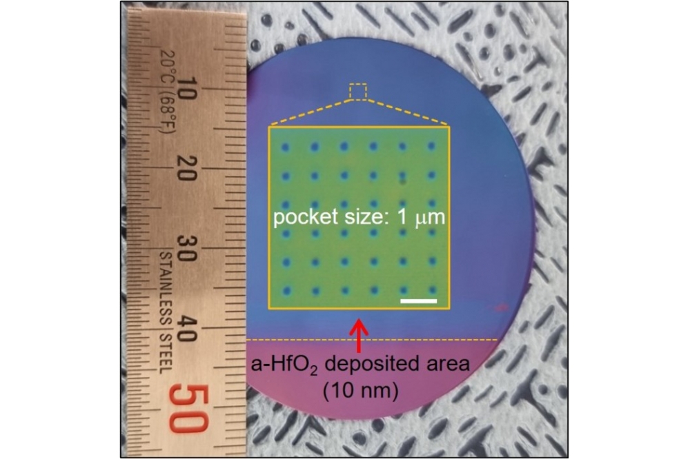
“We designed a geometric-confined structure that facilitates kinetic control of 2D materials so that all grand challenges in high-quality 2D material growth are resolved,” Bae said. “Thanks to the facilitated kinetic control, we only needed to grow self-defined seeding for a shorter growing time.”
The team made another technical breakthrough by demonstrating single-domain heterojunction TMDs at the wafer scale by layer-by-layer growth. To confine the growth of the nuclei, they used various substrates that formed a physical barrier that prevented lateral-epitaxy formation and forced vertical growth.
“We believe that our confined growth technique can bring all the great findings in physics of 2D materials to the level of commercialisation by allowing the construction of single domain layer-by-layer heterojunctions at the wafer-scale,” Bae said.
Bae said other researchers are studying this material at very small sizes of tens to hundreds of micrometers.
“We scaled up because we can solve the issue by producing the high-quality material at large scale,” Bae said. “Our achievement will lay a strong foundation for 2D materials to fit into industrial settings.”
This research was supported by funding from Intel; DARPA (029584-00001 and 2018-JU-2776); and Institute for Basic Science (IBS-R034-D1).


