Precitec launches Flying Spot Scanner

Features include flexible scan trajectories, the ability to measure 12 inch wafers and a Z resolution in the nm range
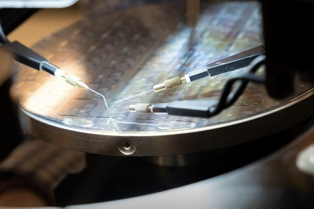
Precitec, a German manufacturer of sensors and optical probes, has launched the ultra-fast Flying Spot Scanner (FSS) 310 for bow, warp, TTV and quality inspection of semiconductor wafers in shorter cycle times. Its features include flexible and highly efficient scan trajectories, the ability to measure 12 inch wafers and a Z resolution in the nm range.
The FSS 310 combines OCT with wide field-of-view scanning and solves the issue of ultra-precise measuring systems normally working very slowly and being extremely expensive. According to Precitec, this scanner’s flexible and fast-moving measurement point within a wide field of view enables non-contact ROI inspection in much reduced cycle times – with no comprises on accuracy.
Thanks to its scan area of 310 mm, the FSS 310 will measure the total thickness variation (TTV), bow and warp of an entire 12-inch wafer and detect any voids in a single scan – and do it in as little as 10 seconds per wafer for standard applications.
The FSS 310 enables a throughput of over 300 wafers per hour (including handling time). The key to such speed is the FSS 310’s in-built scanning system which allows the long paths of linear axes to be replaced by short rotary movements. This significantly reduces measuring times and does away with the need for a precision axis.
When combined with devices from the Precitec CHRocodile 2 IT family, the FSS 310’s fully variable scan trajectories, which the user can program, enable thickness and distance measurements of, for example, Si, doped Si, GaAs and SiC wafers. The FSS 310 can also measure the thickness of semiconductor component coatings (e.g. partial foliation of wafers) as well as measuring the bow of individual dies on wafers prior to further processing.


