
Hydrogen cleaning ensures high-quality mirrors for GaN VCSELs
A flow of hydrogen gas during the growth of distributed Bragg reflectors reduces pits and threading dislocations
A Japanese collaboration is claiming to have made significant progress in the growth of the mirrors for GaN VCSELs. This success could aid efforts to commercialise blue and green VCSELs, which are promising sources for compact and lightweight mobile displays and adaptive headlights with controllable illumination.
The researchers from Meijo University and the National Institute of Advanced Industrial Science and Technology have produced high-quality, n-type AlInN/GaN distributed Bragg reflectors (DBRs) via hydrogen cleaning.
This effort builds on the team’s previous successes in fabricating GaN VCSELs, including the production of variants with non-conductive and conductive AlInN/GaN DBRs that have maximum output powers of 4.4 mW and 2.6 mW, respectively. The addition of doping simplified device design, but degraded morphology, with a rougher surface contributing to a lower output power.
The rougher surface is attributed to a higher dislocation density in the DBR. These imperfections are avoided in the undoped DBR by adding a GaN cap less than 1 nm-thick on the AlInN, prior to an increase in temperature. For the doped DBR there’s a need to introduce a 5 nm-thick AlGaInN compositionally graded layer with a silicon concentration of
6 x 1019 cm-3 to neutralise negative polarisation charges – this must be grown at a lower temperature, leading to a high density of threading dislocations.
As it is not possible to use a higher temperature to reduce the density of threading dislocations, the researchers have tried to supress them by eliminating indium-indium bonds.
“Indium atoms are very volatile,” remarked team spokesman Tetsuya Takeuchi from Meijo University. “If we use hydrogen, it is quite possible to remove indium atoms on the surface.”
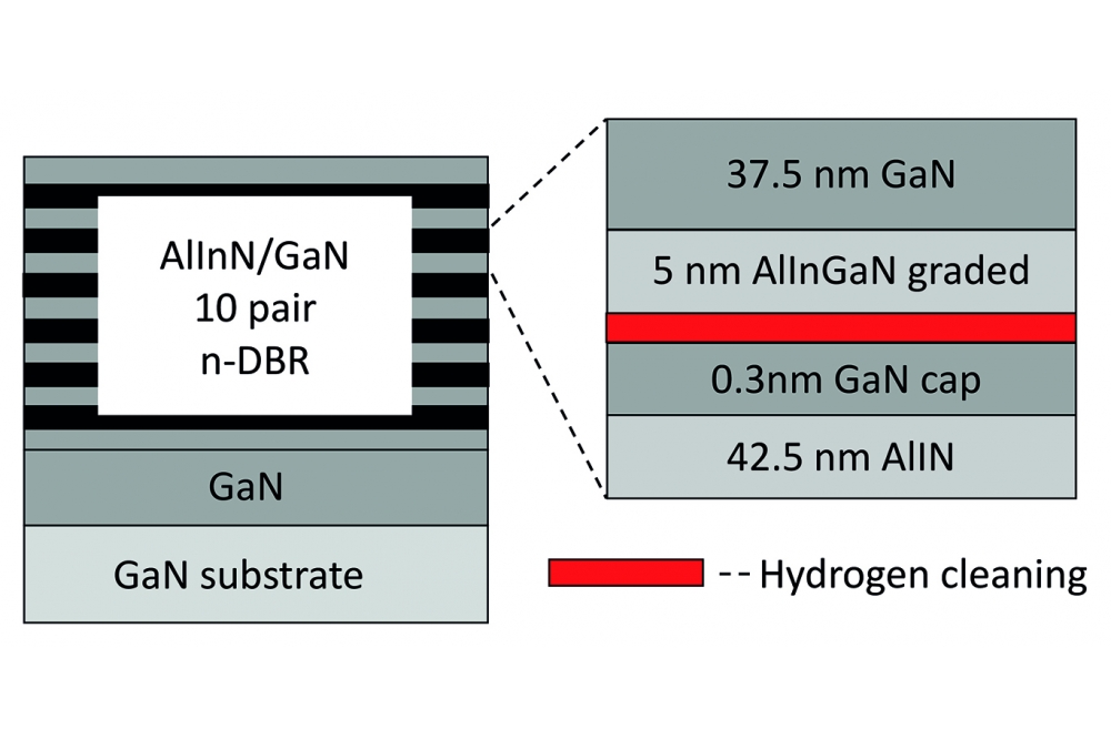
Takeuchi and co-workers began their trials by producing six samples with a 10-period DBR, each grown with different hydrogen flow conditions. The growth of every period of the mirror began with a 42.5 nm AlInN layer and a 0.3 nm GaN cap. Hydrogen cleaning followed during a growth interruption, prior to the addition of a 5 nm-thick AlInGaN layer and a 37.5 nm-thick GaN layer. The growth of the first three layers took place at 840 °C under nitrogen gas; while the 32.5 nm GaN layer was grown at 1100 °C under hydrogen gas.
Variations in hydrogen conditions came from applying a hydrogen flow of 31 standard litres per minute (slm), and varying ammonia flow from 0.5 slm to 4 slm. Assessing material quality by atomic force microscopy (AFM) revealed a minimum pit density of 1.3 x 105 cm-2 for an ammonia flow of 0.65 slm.
The team used this condition to produce a 40-pair, silicon-doped DBR, alongside variants that were undoped and had no hydrogen cleaning.
No pits were observed in the undoped DBR, while doped variants with and without hydrogen cleaning had pit densities of 1 x 107 cm-2 and less than 106 cm-2, respectively. It is even possible that the sample with hydrogen cleaning has no pits.
Additional measurements on the superior doped sample revealed a peak reflectivity of 99.8 percent at 399 nm, and a vertical resistance of 15 W.
These promising results prompt the question of whether it is worth pursuing the growth of GaN VCSELs with two n-type DBRs, plus a tunnel junction that provides a switch from n-type to p-type conduction. However, Takeuchi warns that long growth at a high temperature – it takes 12 hours to grow one DBR – could damage the quantum wells in the active region.
The team are now growing and fabricating GaN-based VCSELs with conducting DBRs, produced using hydrogen cleaning. Takeuchi expects these lasers to exhibit improved performance, due to superior current injection uniformity and a lower device resistance.
Reference
K. Shibata et. al. Appl. Phys. Lett. 15 112007 (2022)


