Loading...
News Article

Repeat microLED order for Solstice S8

News

Order for ClassOne's multi-chamber electroplating system selected for superior process and performance

ClassOne Technology, a provider of advanced electroplating and wet processing tools for microelectronics manufacturing, has received a follow-on order for its Solstice GoldPro gold electroplating system from a leading microLED maker with global manufacturing sites.

Built on ClassOne’s Solstice platform, the system will be used at the customer’s new manufacturing site in Asia for high-volume production of next-generation microLEDs deployed in a range of end applications.

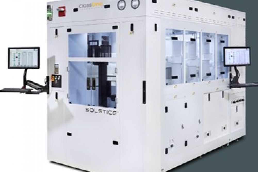
ClassOne’s Solstice S8 system features the company’s proprietary GoldPro plating reactor. Designed to provide efficiency, speed, and improved cost of ownership, GoldPro leverages ClassOne’s fluid motion profile technology to deliver high plating rates and industry-leading plating feature uniformity. The Solstice S8 is on target to ship for installation in the second quarter of 2023.

“Its latest order is evidence of our customer’s success with its existing base of tools, pointing up a significant partnership between ClassOne Technology and this major microLED player,” stated John Voltz, senior vice president of global business operations for the company. “This customer views the Solstice platform’s capabilities as key to accelerating market-readiness for its devices, further validating our world-class single-wafer processing capability and technology leadership in the microLED space.”

According to Allied Market Research, the global microLED market is projected to reach $23 billion by 2030, gaining ground over OLEDs by delivering improvements in brightness, contrast and energy savings.

Available with up to 3, 4 or 8 chambers, the scalable Solstice platform is suitable for both R&D and high-volume manufacturing environments, delivering ultimate wafer uniformity and process control. The system can also accommodate a wide variety of substrates, from traditional silicon devices to compound semiconductors and emerging materials like glass.


SPONSOR MESSAGE

Secure Your Hydrogen Supply

A study supply of high-purity hydrogen is critical to semiconductor fabrication. Supply chain interruptions are challenging manufacturers, leading to production slowdowns and stoppages. On-site hydrogen generation offers a scalable alternative for new and existing fabs, freeing the operator from dependence on delivered gas.

Plant managers understand the critical role that hydrogen plays in semiconductor fabrication. That important job includes crystal growth, carrier gas, wafer annealing, and in the emerging Extreme UV Lithography (EUV) that will enable new generations of devices. As the vast need for semiconductors grows across all sectors of world economies, so does the need for high-purity hydrogen.

Take control with Nel on-site hydrogen generation.

Read more
QD company Quantum Science expands into new facility
Innoscience files lawsuit against Infineon
Riber revenues up 5% to €41.2m
Forvia Hella to use CoolSiC for next generation charging
Photon Design to exhibit QD simulation tool
Ortel transfers CW laser fabrication to Canada
Luminus adds red and blue multi-mode Lasers
PseudolithIC raises $6M for heterogeneous chiplet tech
Mesa sidewall design improves HV DUV LEDs
IQE revenue to exceed expectations
'Game-changing' VCSEL system targets clinical imaging
German start-up secures finance for SiC processing tech
Macom signs preliminaries for CHIPS Act funding
IQE and Quintessent partner on QD lasers for AI
EU funds perovskite tandems for fuel-free space propulsion
EU to invest €3m in GeSi quantum project
Transforming the current density of AlN Schottky barrier diodes
Turbocharging the GaN MOSFET with a HfO₂ gate
Wolfspeed launches Gen 4 SiC MOSFET technology
Report predicts high growth for UK's North East
Element Six unveils Cu-diamond composite
SemiQ launches hi-rel 1700V SiC MOSFETs
Lynred to exhibit Eyesential SWIR sensor for machine vision
Thorlabs buys VCSEL firm Praevium Research
Advancing tuneable InP lasers on a heterogeneous platform
P-GaN gate HEMTs have record threshold voltage
Guerrilla RF releases GaN power amplifier dice
Narrow-linewidth DFB lasers now at 405 and 488nm
Researchers develop tech for future fast-charging stations
Vermont GaN Tech Hub awarded nearly $24M
Onsemi completes buy-out of Qorvo SiC JFET business
Quantum Science announces Innovate UK funding
×
Search the news archive

To close this popup you can press escape or click the close icon.
Logo
x
Logo
×
Register - Step 1

You may choose to subscribe to the Compound Semiconductor Magazine, the Compound Semiconductor Newsletter, or both. You may also request additional information if required, before submitting your application.


Please subscribe me to:


You chose the industry type of "Other"

Please enter the industry that you work in:
 
x
Adblocker Detected
Please consider unblocking adverts on this website