

A national treasure: The UK’s central growth facility
Director of the UK’s national epitaxial facility, Jon Heffernan, discusses its remit, its proficiencies and its contributions to the research and development of compound semiconductor materials and devices.
INTERVIEW BY RICHARD STEVENSON, EDITOR, CS MAGAZINE
RS: Why and when was the national facility founded?
JH: It started in 1979, so we’ve been going for over 40 years. The purpose of the facility is to provide epitaxial materials to researchers across the UK, primarily for UK-funded research grants, but we do work with industries as well.
The idea is that there are many people doing semiconductor research in the UK, but they don’t all have epitaxy facilities. Epitaxy is an expensive technique and it requires significant experience to operate at the highest level and produce semiconductors of the highest quality. Therefore, the EPSRC [Engineering and Physical Sciences Research Council] have funded this facility for many years. It’s part of a network of national research facilities – there are about ten of them – that are centres of excellence.
We’re renewed on a five-year basis. As part of the renewal, there’s what’s called statement-of-need consultations. We go and speak to the community in the UK and ask them what they need from a facility like this. We draw that together, and then it is reviewed by the EPSRC. There’s a competitive call for somebody to run a facility like this and to deliver what the community needs. So we’re very much integrated with what the community is looking for. RS: The facility is more than just the capabilities in Sheffield?
JH: We have two partner universities, Cambridge and UCL. The partners provide specialised materials. We provide a broad range of III-V materials: arsenides, phosphides, antimonides; Cambridge provides gallium nitride material; and UCL provide group IVs and III-Vs-on-silicon.
We also have a pump priming facility, to provide a small amount of initial material to help in supporting grant proposals. In particular we want to support new lecturers. This will help them get their first grants.
We’re now expanding materials to a much wider range, such as 2D materials, gallium oxide. It’s not something that Sheffield could specifically do on its own, because to explore all of these new materials would require many more new reactors, or would require potentially incompatible materials on an existing reactor.
RS: What are some of the biggest highlights over the years?
JH: We’ve tracked and supported the growth of many different technological areas. We’re strongly involved in work on lasers for telecommunications and the internet.
Quantum Technologies is a very big area globally and a big focus in the UK, with the National Quantum Technology Programme. Sheffield has been pioneering many aspects of semiconductor quantum photonics over the last 20 years or so. We have been at the forefront of developing quantum dots to the point where they can be used in quantum technology applications. We have produced some very pioneering results with Toshiba, using quantum-dot-based entangled-photon emitters for quantum communications. We’ve also recently spun out of Sheffield a company working on single-photon sources called Aegiq.
Another interesting emerging area is environmental sensing; in particular using devices in the mid-infrared, including lasers. These types of lasers, particularly quantum cascade lasers, are very challenging to produce. Sheffield was the first group in the world to demonstrate the growth of these type of quantum cascade lasers by MOCVD. That’s quite a big breakthrough in terms of making these types of devices for industrial applications.
We’ve got a number of large projects looking at applications for mid-infrared spectroscopy, using both lasers and detectors. We’re core partners in the EPSRC Future Photonics Manufacturing Hub with the University of Southampton. Funded by EPSRC, it has over 40 companies working with us. Again, we’ve been looking at the manufacturability of devices for mid-infrared applications.
Our partners have done very pioneering work in the growth of III-V lasers on silicon. They’ve demonstrated long lifetimes, compatible with commercialisation.
Cambridge has been working on gallium nitride for many years and has had many breakthroughs. Most recently, they’ve been working on a technology called porous gallium nitride. This is very interesting for display technology, for instance for virtual-reality displays. They’ve spun out a company called Porotech, which has attracted a lot of investment.
RS: How much time do you spend working for academia, and how much time for industry?
JH: It’s difficult to say what the split is as it has varied over the years. I might say about 20 percent industry, 80 percent academia.
Our primary function is to support academic research. The way it works is that somebody applies for a grant to the EPSRC, and if they don’t have their own epitaxy facilities, they come to us and discuss their needs. If the grant is funded, we will supply the epitaxy into that grant.
We work with industry because essentially the capacity of the facility is not taken up entirely with academic research. We also have a remit to work with industry, because of the impact agenda. It’s very important for the UK that publicly funded research does have impact, and that means an impact on the existing industrial sector or starting new companies.
RS: Epitaxial growth technologies are getting more mature, and the systems are getting easier to use. So is the case for a central facility diminishing?
JH: Definitely not. It’s actually the opposite.
At the moment the UK government is looking very closely at investing in the semiconductor industry, and has been consulting very widely over the last year and a half, including with us. It’s now clear to many governments how important semiconductors are – that’s been highlighted by supply chain problems and various geopolitical problems. The US government has just announced the CHIPS act, a $280 billion investment in semiconductor technology. Europe has got its own CHIPS act, and the UK government is expected to announce its intentions fairly soon.
It’s been recognised that semiconductors are extremely important, from an economic impact point-of-view. Semiconductors in general, but III-Vs in particular, are a gift that just keeps on giving. If you track the work that we’ve been doing over the last 40 years, you can see new technologies coming along all the time. There are so many physical properties we can exploit.
Epitaxy is not static, and not really very mature. It still remains very challenging, even classic III-Vs, like indium phosphide, gallium arsenide and the antimonides. We have a very strong expertise in antimonides, which are mainly grown by MBE. Antimonides by MOCVD for production is very immature, but we’re developing it. There’s a long way to go. There are still many areas in III-Vs and in group IV epitaxy where the field is almost completely open.
We continue to get people needing everything from us. EPSRC wouldn’t fund us unless there was an actual demand. Also, if you look more broadly, what is happening in the semiconductor industry, demands and opportunities are just growing by the day.
RS: There are some UK universities, such as Lancaster and Nottingham, that have their own epitaxial tools. For some areas of research – possibly detailed studies of esoteric heterostructures– does it make sense for a research group to have its own tool?
JH: Definitely. The facility that we have is not meant to be the only epitaxy facility in the UK. The reason our facility is set up this way is because there are groups who have their own epitaxy and are pursuing new materials or pursuing epitaxial techniques.
Some of those universities will have invested a significant amount of money to pursue epitaxy. It is an expensive technique and there needs to be a real commitment to this.
If you’re a researcher in another part of the UK and have an interesting idea for a new laser, for instance, it’s actually difficult for you to go to universities and ask them to do that kind of work, especially on a supply basis. If you want to do that, you really need to collaborate with those groups, which means that you have to write joint grants, et cetera, and have to be properly involved in the epitaxy side.
The idea of the facility is that researchers can come to the facility and obtain epitaxial material as a research service. We obviously advise them and work with them on what they want to do, but they can obtain their material without needing to formulate long term collaborations, write joint grants, and be involved in the strategic agenda of the epitaxy itself. That’s the value of the facility.
If you look at the numbers, you’ll see that there are a lot of people interested in semiconductor devices across the UK. Those existing epitaxy groups are not able to cater for that demand, and certainly not able to provide a research service like we just described.
We have a very complementary role with the epitaxy groups in the UK. They’re part of the community. We often help them, and we often advise them – and also people who want to work with them. What we described earlier, in terms of pump priming, is a good example. We’ve now got about six or seven groups that will provide material through the facility and pump priming. They could do that themselves, but the facility has got very good networks in the community. We’ve got long experience of how to manage effectively pump-priming activities that lead to good results.
RS: Is this model of a central facility replicated in other countries?
JH: No. There are probably a handful of big groups with multiple epitaxial tools for producing multiple materials. There’s a few in the US, in places like Santa Barbara, and there’s a few around Europe. But this model for epitaxy, in which we provide materials to a broad range of academics, that’s unique.
We’ve got a steering group that has a number of international members. They are consistently saying that this model is very valuable. They’ve talked a lot about how they’re interested in implementing it in their own countries. It is actually a very good model that the EPSRC has been running over many years.
RS: Do you ever ship material overseas?
JH: Sometimes. Again, it’s the capacity question: do we have capacity to provide material outside of the core function? Generally speaking, we tend to work with UK companies on that front. We often have inquiries, most typically from Europe, and, for example, we’ve done some work for Fraunhofer in Germany. There’s also a Fraunhofer in Strathclyde that we work with on some grants.
RS: Could you explain how the facility is funded?
JH: There’s essentially a block grant from the EPSRC. We are funded on what’s called an 80-20 model, which means that 80 percent of the funding is designed to fund the existence of the facility – the staff employed and keeping the facility available. The rest of the costs of the facility, the 20 percent, is provided through user grants.
It’s actually a good model. It stimulates us to go out and work very closely with the community, in order to have users.
We’re supporting a lot of grants. We typically work with around 25 universities across the UK. We are ISO9001 qualified. That helps us work very closely with industry.
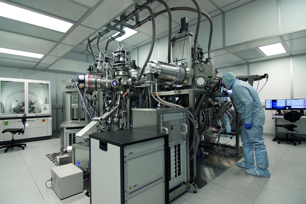
RS: The tools you have include those for MOCVD and MBE?
JH: Yes. In Sheffield, we have three MBEs – we could call it four, because we’ve got one multi-chamber system – and three MOCVD reactors. Cambridge have two MOCVD reactors for nitrides, and UCL has three MBE reactors. So overall it is twelve reactors. We don’t have HVPE.

Two key members of the EPSRC National Epitaxial Facility in Sheffield
are: Ian Farrer (left), Senior Lecturer in Semiconductor Epitaxy and
Materials; and Edmund Clarke (right), Head of MBE Group. Credit: Laure
Divisia.
RS: Amongst those twelve, is there any material system you can’t grow?
JH: Our focus across the consortium is III-Vs and group IV. We can do basically all the III-Vs; in Sheffield we can do arsenides, phosphides, antimonides, and things like dilute nitrides and bismides – novel materials. Cambridge does gallium nitrides, that’s the other III-Vs; UCL is doing the group IV materials. We don’t do materials such as silicon carbide or gallium oxide, but these can be provided through our pump-priming partners. This also includes a whole range of 2D materials that you could explore.
Why don’t we do those materials? One reason is that when we do the community consultation, most people are looking for the III-Vs or group IV. That’s where the biggest need is. Of course, people are interested in other materials, and there are groups now growing them within the UK, but they are not at the point where it should be really provided through a facility model. New materials take a lot of effort. You end up going down a lot of blind alleys before you can make breakthroughs in materials, so it would be very difficult and very expensive for a central facility like ours to offer all kinds of new materials. Typically, you also need dedicated reactors, because you’ve got all kinds of material incompatibilities. Where would be the users to support those reactors?
We have had discussions with the community, the epitaxy groups involved, the EPSRC, and our steering group. In terms of new materials, the facility has a role to play: to support the development of those new materials until they reach a point of maturity where there’s enough users in the UK that may want the central facility for that.
For materials like gallium oxide, silicon carbide, or some of these II-VI materials, it may be that in five years’ time there are so many people working on this technology within the UK that to deliver it through a central facility makes sense, both academically and financially. But we’re not at that point with those materials. There’s a risk of investing in a central facility to provide a huge range of materials, some of which there won’t be the users to actually develop the research.
RS: How do you characterise the material you ship?
JH: We’ve got extensive characterisation facilities within each of the three organisations. There’s a core set of characterisation techniques that are actually part of our ISO9001, which ensures that what we deliver meets the specifications of the user. For instance, we will always do X-ray measurements on material to check that the material quality is good. We always do Normarski to check that the surface quality is good. These are indications of whether the growth has worked or not. With optical devices, we will do the photoluminescence, because we need to see that light actually comes out. We have all kinds of characterisation techniques that we need for basic materials.
What we don’t have is some of the more advanced, specialised, expensive characterisation, like advanced transmission microscopy, for instance. But we outsource that kind of work.
Having the equipment is one thing. We’ve got 40 years’ experience characterising materials as well. That’s a big part of the facility. It’s not just our epitaxy capability; it’s our knowledge of materials and our knowledge of how to characterise and understand them that is very valuable. We often get users who have a fairly poor understanding of what they’re asking for. People may want to combine materials, for instance, but they haven’t even thought about lattice matching. So our knowledge of the materials is also very important for users.
RS: How long does it take you to ship material?
JH: It depends on the complexity of the material. We primarily support people on grants, so all of our work is peer reviewed. People come to us looking for material, we then supply them with essentially a quote, which goes on to their grant. We will provide the material if the grant is funded.
We’re doing new research; we’re not providing off-the-shelf material because that’s not our role. If somebody looks for off-the-shelf material, we will encourage them to find commercial suppliers. Typically, we have to deliver requested wafers within a three-month period.
Some other projects are really pushing materials development or pushing the device concept. That can take longer, typically several iterative cycles.
Although we’re a research service, we effectively work collaboratively. Users need to work with us, understand the limitations, the constraints, et cetera. We will do quite a lot of characterisation before delivering the final product to the user.
RS: For wafers that are used by industry, can you support up to prototype production?
JH: We can, but our main constraint on that front is volume. We don’t produce wafers in any kind of volume. We could, but it would take the capacity of the facility.
We can produce wafers up to a high TRL, if that’s what you mean, in terms of prototyping. We have certainly produced lasers that have been used in the field, deployed in systems for various companies. But our primary role is to deliver to academic researchers.
While the EPSRC National Epitaxial Facility may be renowned for its growth via MBE, it also has MOCVD tools, including two Aixtron reactors. Credit: Zofia Bishop
Recent research highlights involving contributions from the UK’s National Epitaxial Facility
“A prototype AlInP electron spectrometer”, M.D.C. Whitaker et al. Planetary and Space Science 205 105584, (2021) Development of a particle counting electron spectrometer using an AlInP photodiode, useful for space science
missions where the instruments would be subject to high temperatures and intense radiation.
“Continuous-wave quantum dot photonic crystal lasers grown on on-axis Si (001)”, T. Zhou et al. Nature Communications, 11 977 (2020) III-V membrane photonic crystal lasers monolithically grown on CMOS-compatible on-axis silicon substrates, for applications in on-chip photonic networks.
“Quantum interface of an electron and a nuclear ensemble”, D A Gangloff et al. Science 364 (2019) Coherent manipulation of nuclear spins in a quantum dot, using interactions with an electron, forming the basis for development of an interface to a long-lived solid-state quantum memory.
“High Purcell factor generation of indistinguishable on-chip single photons”. F Liu et al. Nature Nanotechnology 13835 (2018)Generating single photons with high indistinguishability by placing a quantum dot in a photonic crystal cavity that
considerably shortens the radiative lifetime of carriers in the dot, enabling on-chip single photon sources with very high repetition rates.
“A quantum LED for the standard telecom window around 1550 nm”, T. Müller et al. Nature Communications 9 862 (2018)Demonstration of a light emitting diode emitting single photons and entangled photon pairs around the 1550 nm telecom window, for long-distance fibre-based quantum communications and cryptography.
"Wafer-scale Fabrication of Non-Polar Mesoporous GaN Distributed Bragg Reflectors via Electrochemical Porosification”, T. Zhu et al. Scientific Reports 7 45344 (2017) Demonstration of non-polar GaN distributed Bragg reflectors formed from layers of non-porous and porous GaN using a novel electrochemical porosification step that allows realisation of DBR structures on a wafer scale.
“Phase-locked indistinguishable photons with synthesized waveforms from a solid-state source” C. Matthiesen et al. Nature Commun. 4 1600 (2013) Showing how the waveforms of indistinguishable single
photons from a quantum dot may be controlled using resonance fluorescence techniques. Enables a variety of quantum technology applications.


