Loading...
Listen to this article
News Article

Ams Osram qualifies Aixtron tools for Micro LEDs

News

AIX G5+ C and G10-AsP MOCVD systems now qualified on 200mm wafers for a Micro LED application

Aixtron has announced that Ams Osram has qualified the Aixtron AIX G5+ C and G10-AsP MOCVD systems on 200mm wafers for a Micro LED application.

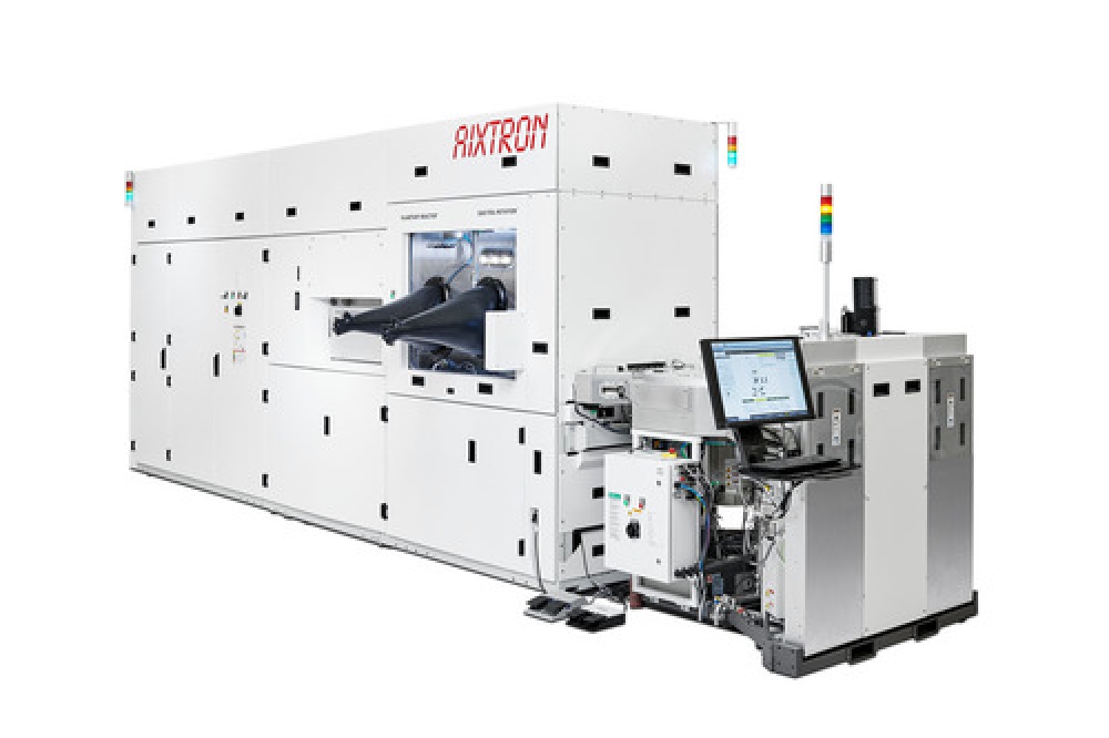
The MOCVD systems AIX G5+ C and the new G10-AsP from Aixtron SE offer Aixtron planetary technology which is said to be paving the pathway for the next generation of high-resolution Micro LED displays.

In spring 2022, Ams Osram had announced plans to create additional manufacturing capacity in 200mm for the production of LED and Micro LED at its existing location in Malaysia. The MOCVD systems are expected to help enable volume production of Micro LED for a new generation of display applications.

“Aixtron and Ams Osram have a long-standing cooperation, and we are familiar with the performance and quality standards of the equipment. For an ambitious project like the development and production of Micro LED for AsP and GaN devices, we needed exactly such a partner at our side”, says Robert Feurle, executive VP and head of Business Unit Opto Semiconductors at Ams Osram.

Felix Grawert, CEO and president of Aixtron SE, adds: “The G10-AsP and AIX G5+ C qualification at Ams Osram is a very important milestone in our company’s history. Ams Osram is a world-class LED manufacturer and perfectly positioned to enable the fundamental new technology that will come to market. We are on the verge of a technology shift away from conventional display technologies to a new type of Micro LED displays. Now, Aixtron is entering one of the future’s growths markets that has an enormous potential, and we are doing this with a perfect partner at our side.”

The production of Micro LED comes with special requirements, including a special transfer process where multiple thousands of LED chips (arrays) are picked up and transferred. Any defect can result in dead pixels that can make an entire array useless. Hence, an almost error-free epitaxy process is necessary, minimising defects and allowing for high yield and economically viable production of Micro LED.

Aixtron’s new G10-AsP epitaxy tool has been designed to address the specific needs of this application: It is a fully automated AsP reactor offering cassette-to-cassette wafer loading as well as a cleaning mechanism based on in-situ etching. Together, these two features have a major impact on the yield performance, says the company.

SPONSOR MESSAGE

Secure Your Hydrogen Supply

A study supply of high-purity hydrogen is critical to semiconductor fabrication. Supply chain interruptions are challenging manufacturers, leading to production slowdowns and stoppages. On-site hydrogen generation offers a scalable alternative for new and existing fabs, freeing the operator from dependence on delivered gas.

Plant managers understand the critical role that hydrogen plays in semiconductor fabrication. That important job includes crystal growth, carrier gas, wafer annealing, and in the emerging Extreme UV Lithography (EUV) that will enable new generations of devices. As the vast need for semiconductors grows across all sectors of world economies, so does the need for high-purity hydrogen.

Take control with Nel on-site hydrogen generation.

Read more
QD company Quantum Science expands into new facility
Innoscience files lawsuit against Infineon
Riber revenues up 5% to €41.2m
Forvia Hella to use CoolSiC for next generation charging
Photon Design to exhibit QD simulation tool
Ortel transfers CW laser fabrication to Canada
Luminus adds red and blue multi-mode Lasers
PseudolithIC raises $6M for heterogeneous chiplet tech
Mesa sidewall design improves HV DUV LEDs
IQE revenue to exceed expectations
'Game-changing' VCSEL system targets clinical imaging
German start-up secures finance for SiC processing tech
Macom signs preliminaries for CHIPS Act funding
IQE and Quintessent partner on QD lasers for AI
EU funds perovskite tandems for fuel-free space propulsion
EU to invest €3m in GeSi quantum project
Transforming the current density of AlN Schottky barrier diodes
Turbocharging the GaN MOSFET with a HfO₂ gate
Wolfspeed launches Gen 4 SiC MOSFET technology
Report predicts high growth for UK's North East
Element Six unveils Cu-diamond composite
SemiQ launches hi-rel 1700V SiC MOSFETs
Lynred to exhibit Eyesential SWIR sensor for machine vision
Thorlabs buys VCSEL firm Praevium Research
Advancing tuneable InP lasers on a heterogeneous platform
P-GaN gate HEMTs have record threshold voltage
Guerrilla RF releases GaN power amplifier dice
Narrow-linewidth DFB lasers now at 405 and 488nm
Researchers develop tech for future fast-charging stations
Vermont GaN Tech Hub awarded nearly $24M
Onsemi completes buy-out of Qorvo SiC JFET business
Quantum Science announces Innovate UK funding
×
Search the news archive

To close this popup you can press escape or click the close icon.
Logo
x
Logo
×
Register - Step 1

You may choose to subscribe to the Compound Semiconductor Magazine, the Compound Semiconductor Newsletter, or both. You may also request additional information if required, before submitting your application.


Please subscribe me to:


You chose the industry type of "Other"

Please enter the industry that you work in:
 
x
Adblocker Detected
Please consider unblocking adverts on this website