
Eradicating dark-line defects in deep-UV laser diodes
A sloped mesa geometry promises superior deep-UV laser diodes by banishing dark-line defects
A team from Japan has eliminated dark-line defects in aluminium-rich, AlGaN-based lasers by introducing a sloped mesa geometry. Eradicating these defects should enable the production of more reliable, higher efficiency laser diodes emitting within the UVC, which spans 100 nm to 280 nm.
According to the engineers from Nagoya University and Asahi Kasei Corporation, today’s AlGaN UVC lasers are impractical, due to their low efficiency, short lifetime and lack of reliability.
Contributing to these weaknesses are dark-line defects, which deteriorate the active area at the edge of the mesa. One workaround is to place the p-type electrode away from the mesa edge, so the current path avoids this area – but this leads to a higher resistance, and in turn device heating and a hike in threshold current.
Adopting this approach, the team recently produced a 272 nm laser delivering CW operation at 5 °C. For this 600 µm-long laser, every 5 µm increase in distance from the mesa corner increased the resistance between the n- and p-electrodes by 2.6 W. The high resistance that resulted led to
Joule heating, which prevented room-temperature lasing. The engineers could not reduce this resistance by thickening the Al0.75Ga0.25N n-type cladding layer or decreasing its aluminium content due to constraints associated with pseudomorphic growth. Breaking these rules would lead to a higher defect density in the active region, quashing radiative recombination.
One of the weaknesses of the team’s 272 nm laser is that it is riddled with dark-line defects. To investigate their origin, the team’s latest work involved MOCVD growth of a laser structure on a single-crystal AlN substrate. This heterostructure consisted of: a 350 nm-thick n-type Al0.7Ga0.3N cladding; a 100 nm-thick Al0.63Ga0.37N waveguide with multiple quantum wells; a 320 nm-thick p-type cladding layer, with distributed polarization doping and an average aluminium content of 85 percent; and a p-contact layer. Dry etching isolated the p-contact layer and defined a mesa stripe along the [1100] direction.
To aid analysis, the team avoided adding metal electrodes to their device. However, they still applied thermal treatments that would be used during the fabrication of metal electrodes to their epistructure, in case this influenced its material quality.
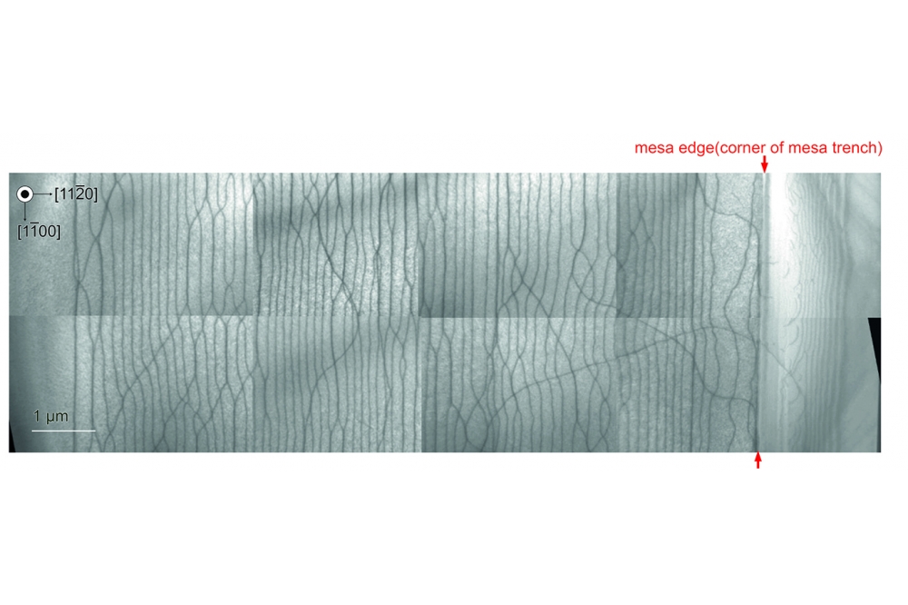
Plan-view transmission electron microscopy images of this structure clearly show dark-line defects (see figure), observed as far at 12 µm inside the mesa edge. Inspection of these images reveal an absence of partial dislocations and stacking faults, providing strong evidence that the dislocations stem from slip, resulting from forces perpendicular to the mesa stripe.
These dislocations occur in other material systems, such as InGaN/GaN and AlN/SiC heterostructures, where there is a large strain due to lattice mismatch, with symmetry of the plane stress broken by the mesa trench.
Finite-element modelling by the team revealed the forces acting within the structure, and indicated that reducing the mesa slope angle to less than 50° could provide a significant reduction to the shear stress concentration at the corner of the mesa trench.
The team have put this finding to the test. “AlGaN has a slow etching rate, so we were worried whether we could obtain the desired shape,” admitted team spokesman Maki Kushimoto. “However, after trying several resist and reflow conditions, it is clear that we can form the mesa stably.”
According to plan-view transmission electron microscopy, structures with a slope inclination of 15° to the surface are free from dark-line defects.
Goals for the team include further studies of dislocations. “I would like to clarify the mechanism of dislocation propagation to the active layer, the effect of thermal expansion, and the effect of crystal plane orientation,” revealed Kushimoto.
Pictured above: Plan-view transmission electron microscopy reveals dark line defects in AlGaN laser diodes with a conventional geometry.
Reference
M. Kushimoto et al. Appl. Phys. Lett. 121 222101 (2022)


