

Now’s the time to commercialise the GaN IC
Power ICs that combine several power electronics functions in a single
GaN chip are set to play a major role in worldwide electrification.
BY GERALD AUGUSTONI, PLINIO BAU, DOMINIQUE BERGOGNE, FLORIAN COUVIN AND RYM HAMOUMOU FROM WISE INTEGRATION
Power Conversion Systems are at the heart of most electronic equipment, from home appliances and laptops to data centres and electric vehicles. In some of these applications GaN technologies will soon be essential, because silicon has hit its physical limits as a power-conversion platform.
As well as increasing the efficiency of power conversion stages, GaN has other virtues. They stem from its great physical properties, such as: a bandgap of 3.2 eV, nearly three times that of silicon; and a breakdown field of 3.3 MV/cm, which is around ten times that of silicon. These strengths contribute to excellent values for both the on-resistance and the key figure of merit – the product of the on-resistance and the surface area of the chip. GaN devices can deliver high currents, a high breakdown voltage and a high switching frequency, and are competing with current MOSFETs and super junction MOSFETs in power applications operating at voltages of up to 650 V.
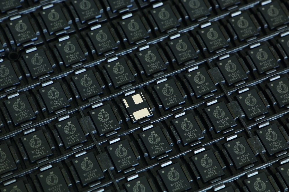
Traditionally, power designers build half-bridge circuits that serve in power conversion systems from discrete transistors and a number of external components, such as drivers, level shifters, sensors, bootstraps and peripherals. Improvements can be realised by combining discrete GaN devices, rather than those made from silicon, with other components. However, there is a better approach than this – one that we are pursuing at Wise Integration, which is based in France. Founded in 2020, our team is pioneering the GaN power IC, which combines several power electronics functions in a single GaN chip. Through integration, we are improving speed, efficiency, reliability and cost-effectiveness.

More agile adapters
Over the past decade, major OEMs have devoted much effort into making the most powerful smartphones, the thinnest notebooks and the largest TVs. The common factor in this trend is the growing demand for power, to enable sharing of a massive amount of data every second.
Unfortunately, OEMs have not been paying much attention to the adapters placed next to their products. This has resulted in bulky, heavy, inefficient power supplies that rely on silicon transistors. But that is starting to change.
Back in 2019, GaN technology penetrated the consumer market, initially in 30-100 W adapters. Since then this wide bandgap technology has spread widely, evolving as a next-generation power-conversion option. Today, most makers of mobile devices acknowledge that adapters are part of the equation, with mobility requiring them to be compact and lightweight, in tune with their main product strategy. Power supplies are now becoming an integral part of the product.
Power density is the main ‘driver’ for GaN, while efficiency is becoming increasingly important to meet new demand for AC-DC/DC-DC power supplies from 100 W to 3 kW, especially for the data-centre industry. For this specific market, higher power is required in the same form factor to reach high levels of efficiency.
GaN had a great year in 2022. Along with its growing popularity it became cost competitive, with expanding demand prompting several global foundries to add GaN lines. At the system level, it will not be long before AC-DC analogue controllers are ‘GaN compatible’. However, their GaN capabilities will not be fully utilised, because they are still switching at low frequencies.
Now is the time for the GaN industry to start overcoming this limitation and deliver the next big energy and power boost. This can come from a move from discrete GaN devices to GaN ICs that deliver a hike in efficiency at the system level, and lead to material costs that are more competitive than traditional silicon-based power supplies.

Figure 2. Integrated half-bridge transistors composed of a low-side and a high-side power switch in the same package.
GaN IC design
To see this vision fulfilled, we have been prototyping different HEMTs, using different form-factor and metallisation strategies. Our efforts have involved the modelling and design of GaN transistors for 100 W to 1 kV applications using multi-project wafers. These investigations have drawn on expertise at CEA-Leti, the French microelectronics research institute. Through this collaboration we have obtained a solid basis for mass production.
Among all the multi-project wafers and prototypes we have built, we have undertaken R&D projects that are focused on power transistor layout topologies. From matrix metallisation to comb metallisation, we have uncovered parasitic contributions from the metal paths that affect performance parameters, leading to different values for parasitic capacitance, on-resistance and gate internal resistance. We have found that the pad positioning in the floorplan diagrams impacts the parasitic on-resistance caused by the bonding wires, as well as the distribution of current and metal resistance calculated by metal squares. Changing the bonding wires’ position in the power IC floorplan impacts the final on-resistance in two ways: post-layout simulation and performance parameters change, due to variation in current distribution inside the metallisation; and the addition of bonding wires in parallel impacts the final resistance. Over the past two years we have built hundreds of prototypes, selecting the best ones. We have also performed electrostatic discharge (ESD) tests on: prototypes for different circuit strategies, circuits with diodes, digital input/output clamp and power clamp circuits.
When our community gathers at international conferences, along with discussions of power transistors, there are conversations related to analogue circuits for GaN power integration. To obtain high-performance circuits, it is clear that there’s a need to overcome fabrication-corner dispersion and a charge-trapping effect. Another impediment is the absence of p-type transistors for pull-up circuits. However, designers can overcome these challenges by adapting their circuit topologies. Many have demonstrated analogue circuit blocks, such as voltage reference, under-voltage lock-out, ESD circuits, comparators and operational amplifiers, with high switching frequencies of up to 10 MHz. These blocks are also compatible with voltages up to 650 V and powers of up to 1 kW.

Figure 3.Typical GaN-based power supply with analogue control.
System-level benefits
An entrenched factor that limits the performance of systems that employ silicon MOSFETs is the figure of merit for this transistor – it is the product of its on-resistance and the combination of its internal gate-to-source and gate-to-drain capacitance. Moving from silicon to GaN allows designers to enjoy a far better figure-of-merit. There’s no longer a limit to the operating frequency, which can be ten times that of silicon.
However, it’s not as simple as it first appears, as there’s another obstacle to raising the system frequency. If the GaN transistor in the converter is not operating in a soft switching condition – that’s the situation where the voltage at every turn-on of the transistor is close to zero, or otherwise limited – the energy stored due to the capacitance of transistor, as well as the system capacitance, has to be dissipated in GaN, causing the transistor to quickly overheat. While this may be acceptable for systems operating at 100 kHz or below, it is not for frequencies from 500 kHz to 2 MHz, the typical operating frequencies of our systems.
Our solution is to constantly operate in a soft switching condition, accomplished by specific control and topologies. To ensure that this is possible for everyone, we have launched WiseWare controllers (see Figure 4).

Figure 4. WiseWare 1 digital control.
Driving forces
The GaN IC is destined to be the next step on the road to high power density and system integration, two of the key drivers behind the historical success of semiconductors. But power electronics, and power transistors in particular, have lagged in integration, held back by the complicated processes employed for forming vertical architectures.
We are in no doubt that the integration offered by our GaN lateral process will deliver benefits at the system level. Realising integration is a crucial step forward, as it always enables a reduction in system dimensions and an increase in complexity, which improves reliability and performance.
Our GaN ICs will bring benefits to market, because they enable: a shrinking of system dimensions, by reducing the number of components and minimising power losses, which leads to practical packaging for heat transfer; increased complexity, which can lead to optimised system performance, including better shaping of the power signal; improved reliability, thanks to fewer components on the board, and additional system protection that includes early detection of abnormal conditions; and better performance with faster switching devices, thanks to driver integration. The latter enables a higher operating frequency, by reducing parasitic components and ensuring better switching behaviour. In addition, there is the opportunity to introduce ‘in-power sensing’, to feed the true status of the converter back to the controller through sensors integrated on the power transistor die.
Of course, this evolution requires several steps. However, such efforts are worthwhile, as they provide the main driving force to the future of the GaN market. While progress may span several decades, the result will be a revolution in system design, so that it delivers unmatched performance at low cost.

Figure 5: WiseWare 2 digital control.
Digital control
Digital GaN is a promising option for realising great performance with GaN ICs. It is a disruptive approach to digital control. No longer are analogue signal blocks ‘translated’ into digital blocs, while the functions of the GaN IC and digital GaN controllers are partitioned in such a way that each part boosts the other part’s performance. Current sensing is usually complex to achieve, but the digital GaN solution makes the analytical estimation of the current possible, thus creating a virtual current sensor. Such a sensor, which costs only lines of code, prevents losses, saves PCB area, reduces the bill of materials and eliminates analogue sensor problems (see Figure 5).
Another advantage of digital GaN is that it elevates high resolution pulse-width modulation to a level that cannot be reached with analogue controllers. By opening up the opportunity for a precise sub-nanosecond timing resolution, combined with high-performance microcontroller units (MCU), new solutions are introduced for zero-voltage switching – this is a technique that reaches extreme high switching frequencies without increasing switching losses, thanks to what is called ‘soft switching’. By computing exact switching times, a digital GaN controller can perform zero-voltage switching using low-bandwidth hungry sensors and a model of the switching device.
Note that the high-frequency, switched-voltage waveforms are not measured or sensed. Instead, slow-changing variables are fed to the MCU analogue-to-digital conversion peripheral.
Digital GaN opens new pathways from the power stage to the cloud, helping to combat climate change by drastically reducing the amount of data exchanged. Sitting at the heart of power supply units and power converters, digital GaN can aggregate performance data from the power circuits to compute health-and-usage data. An ultralow bandwidth data flow can be generated by processing the data onboard: it requires just a few kilo-bytes per day to provide optimal information for monitoring huge installations using a massive quantity of power supply units.
By providing an intelligent link between the world of data and the world of electrical power, digital GaN enables remote-firmware updating, as well as feature activation over the internet. This possibility is common in many computing devices, such as internet boxes, TVs and computer mainboards. There is also the opportunity to deliver power and data to EVs.
For power supply systems that serve data-hungry needs that are as diverse as consumer electronics, e-mobility, data centres and industrial applications, there will be increasing pressure to deliver the vast amounts of power required to transmit that data. Helping to meet that demand are our GaN ICs that combines several power electronics functions in a single GaN chip. The payoff: improved speed, higher efficiency, greater reliability and cost-effectiveness, alongside a digital control that opens new paths from the power stage to the cloud, while respecting the environment by drastically reducing the amount of data exchanged.
Further reading
† P. Bau et al. “Static and dynamic measurements for GaN integrated switches”, International Exhibition and Conference for Power Electronics (PCIM 2022)
† D. Bergogne et al. “Integrated GaN ICs, development and performance” 21st European Conference on Power Electronics and Applications (EPE’2019)


