Scrutinising SiC with X-ray topography
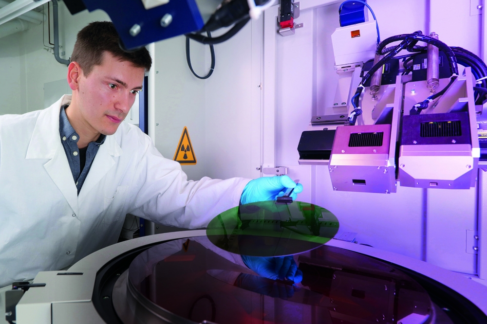
X-ray topography, already on the cusp of revolutionising the quantification of dislocations in SiC wafers, is now available in a high-throughput form that accelerates progress.
BY CHRISTIAN KRANERT AND CHRISTIAN REIMANN FROM FRAUNHOFER IISB AND SHINTARO KOBAYASHI, YOSHINORO UEJI, KENTA SHIMAMOTO AND KAZUHIKO OMOTE FROM RIGAKU
Silicon carbide is now a mature material that enjoys substantial success in the power electronics sector. Devices made from this semiconductor are currently displacing silicon-based incumbents, especially in the fast-growing market of electric mobility, where SiC is being adopted in both vehicles and charging infrastructure.
Alongside ramping sales of SiC devices, there has been a tremendous improvement in the quality of the material, as well as increases to wafer diameter to 150 mm and 200 mm. However, when it comes to crystalline material quality, SiC is certainly not as perfect as silicon.
One of the weaknesses of SiC is that it contains dislocations. These imperfections are not going to completely vanish from this material in the short term, and their presence matters – they can have a severe impact on the yield, the performance and the reliability of the final devices. Due to this, there’s a need to know the dislocation density of a SiC wafer, a metric that reflects the quality of the material. In fact, such information is more prised than ever, because the high standards within the automotive industry are pushing supply chains towards a complete tracking of all components, from raw material to the final product. Consequently, characterising dislocations in the substrate material provides a valuable piece of information for qualifying suppliers, and for tracking device failure.
Figure 1. Typical TSD density mapping obtained with the Rigaku XRTmicron. Red circles indicate automatically detected locations of screw dislocations.
Until recently, the ‘gold standard’ for quantifying dislocations in SiC substrates involved etching this material in an aggressive alkaline melt heated to roughly 500°C. But this approach is far from ideal. One major weakness is that it is destructive to epi-ready wafers. As every SiC boule may differ from the next, wafer manufacturers analyse at least one wafer from every boule to ensure that they meet the required specifications. Assuming an average yield of 30 to 40 wafers per boule, this etching-based evaluation incurs a yield hit of around 3 percent, a loss that could be eradicated with a non-destructive characterisation technique. Additional drawbacks include those related to the stability of the etching process, the reliability of automated etch pit counting and a lack of standardisation.
Addressing all of these concerns is high-resolution, lab-scale X-ray topography (XRT). This technique builds on synchrotron XRT measurements, which have always been used to identify and detect dislocations – but those measurements are typically performed only locally, and require beam time at synchrotron facilities, so are unsuitable for use in an industrial setting.
These limitations make the Rigaku XRTmicron, which brings high-resolution XRT to the lab, a game changer. This instrument allows engineers to visualise single dislocations, thus making it possible to quantify them. As dislocation images recorded by XRT originate purely from local crystallographic strain, this technique is not derailed by variations in doping concentration between different wafers.
Figure 2. Pushing the limits of accuracy: Three neighbouring wafers from the same crystal were measured by XRT on both sides, and the average TSD density over the wafer area taken. As well as resolving the decreasing trend of dislocation density from seed to dome, the data reveals which face of the wafer is facing which direction. One might even estimate the spacing between the individual wafers.
While these advantages have much promise, those within the SiC industry seek assurance that the results provided by this non-destructive technique are consistent with those that come from etching. Investigating whether this is the case is our team at the Centre of Expertise for X-ray Topography, a research collaboration between Rigaku Corporation and Fraunhofer IISB. We address market needs by drawing on Rigaku’s excellence in building state-of-the-art X-ray tools and Fraunhofer IISB’s competences along the SiC value chain.
We have found that once those working in industry have been assured of the validity of XRT, their interest in this technique rapidly increases, along with demands, particularly regarding measurement times. To address this specific demand, we have introduced the FastBPD approach: it brings high-speed, full-wafer XRT measurements to labs and industry lines. But let’s start this story at the beginning…
From TSDs…
The most common polytype of SiC substrate is the 4H variant, which is usually grown by physical vapour phase technology. The material that results contains various defects with different properties. Historically, 4H-SiC contained large volumetric defects, like polytype inclusions, but now they tend to be eliminated completely from prime grade material. Unfortunately, micropipes and stacking faults are still present, leading to almost certain device failure. However, the propensity of these imperfections has plummeted in recent years – and for R&D purposes, the presence of these extended defects can be spotted easily by the naked eye in X-ray topograms.
This leaves us with three common types of dislocation: threading screw dislocations (TSDs), threading edge dislocations (TEDs) and basal plane dislocations (BPDs). With the conventional approach to identify these dislocations, standard potassium hydroxide etching of the silicon-face of SiC substrate material, etch pits from TSDs and TEDs are not easily distinguished. Since today’s prime grade material has far fewer TSDs than TEDs, it is a challenge to determine the TSD density reliably. To overcome this issue, technicians can turn to C-face etching, or add oxidising agents to the potassium hydroxide melt. But this introduces new challenges. The reality is that the SiC world has lacked a technique to reliably quantify the TSD density in substrates, often resulting in the omittance of TSD densities in industrial wafer specifications.
An absence of data for the TSD density matters, because this class of dislocation can wreak havoc in some type of device. For example, if TSDs are present in the channel region of MOSFETs, this can promote electric breakdown, leading to device failure. Another issue is that depending on epitaxial conditions, growth pits can occur at the locations of the TSDs, creating device processing issues and ultimately causing device failure.
For the detection of TSDs, XRT is peerless. With correct diffraction conditions, the topographic image almost exclusively exposes individual dark spots, each corresponding to a single TSD (see Figure 1). Simply counting these spots provides the density of TSDs. However, those working within industry have had to be convinced of the capability of XRT before they are willing to make the switch to this technique. They have required reassurance of how the results by XRT relate to those realised by etching, and they needed convincing of the reliability and the accuracy of defect detection.
We have undertaken tests to evaluate how XRT compares against five other experimental techniques. Our goal was to verify that counting based on XRT contrast delivers the same information as conventional approaches.
The five other experimental techniques were: examining etch pits after epitaxy, which allows one to distinguish between TSDs and TEDs; inspecting etch pits, following etching in a melt of potassium hydroxide and sodium peroxide; counting hillocks on the C-face of SiC after etching in potassium hydroxide; using grazing incidence synchrotron XRT, as this can identify TSDs; and scrutinising growth pits after epitaxy, an approach that allows engineers to relate material imperfections to weaknesses associated with device processing. All five comparisons affirmed the capability of XRT, with tests yielding identical dislocation distributions, numbers, and positions. Based on this overwhelming agreement, we are in no doubt whatsoever over the validity of XRT measurements for TSD detection.
If XRT is to be used in industry, tools that apply this technique must deliver reliable results. To confirm that this requirement is met, we developed a measurement and analysis routine – this included measurement parameters, guidelines for the required image quality, and a robust but fast analysis algorithm, which required less than 5 minutes to analyse the full topogram of a 150 mm wafer. We have found that our instruments provided a high measurement repeatability, giving values within 3 percent of one another, and an inter-machine reproducibility with a similar error. Drawing on this exceptional degree of accuracy, engineers can even measure differences in TSD density between neighbouring wafers (see Figure 2).
The opportunity to undertake non-destructive measurements awakens a desire to measure more wafers per SiC boule. However, if this is to happen, there needs to be an increase in throughput. To ensure this is possible, we have adapted partial wafer measurements to the XRT approach. Thanks to this refinement, one can measure the average TSD density of a full 150 mm within 30 minutes with an error of less than 10 percent.
This chapter of this particular story culminated with the publication of SEMI M91, an industrial standard describing TSD detection by XRT. This documentation ensured that XRT is now an established tool for dislocation detection and, in the case of TSDs, has overtaken the old de-facto standard by becoming a regular alternative.
Figure 3. Typical X-ray topograms in transmission geometry, mainly
showing basal-plane dislocations as curvilinear features. Sub-figures
show different dislocation densities, increasing from left to right. A
measurement of individual lines is only possible at low dislocation
densities, those below 500 cm-2 (left image). A different
analysis strategy is required for higher dislocation densities. Using
integral image analysis, this limitation has been overcome, allowing the
measurement of very high BPD densities of 5000 cm-2 and above.
…over BPDs…
For companies working with SiC substrates, the opportunity to undertake non-destructive detection of TSDs is a compelling reason to invest in XRT for material characterisation. But that is not the only benefit: there is also the detection of other types of defects, including BPDs.
With XRT, it is more challenging to quantify the detection of BPDs than TSDs, because it is more complex than simply counting points. BPDs appear as lines in the topogram, and they start to overlap at moderate densities, due to their extended shape. Thus, it is hard to tell where one BPD starts and another ends (see Figure 3).
Another impediment is that the visibility of BPDs using surface-sensitive measurements in a reflection geometry is poor, even for extremely long measurement times. Thus, switching to a transmission geometry is beneficial from a measurement point of view, but brings another challenge: then it is not clear whether a single BPD actually intersects with the interface, resulting in an etch pit.
We overcame these problems with a calibrated, integral approach. Rather than trying to measure the length of visible lines or count them, not knowing whether or not they intersect with the surface, we pursued an approach where we start by analysing local areas and generating a value of arbitrary unit for each region. We have shown that the values we obtain are proportional to the actual BPD density, measured by etch pit counting. Thanks to this relationship, a calibration curve allows us to generate BPD density mappings that reproduce the corresponding BPD etch pit density very well.
Again, industry acceptance has required proof of the accuracy of our new technique. Helping with this endeavour are our findings from a study of wafers from almost all major SiC manufacturers. After XRT measurements, we undertook potassium hydroxide etching on all these wafers and discovered some wonderful news – the calibration curve is the same for all manufacturers. The implication is that the calibration curve of one wafer can be used for evaluating another. Therefore, the calibration procedure only requires an initial calibration with a single, suitable wafer, or possibly a small set of them. Afterwards, the calibration curve can be used over and over again. Drawing on this, we have determined that the accuracy of the BPD density is more limited by the quality of the etch pit data used as input for calibration than by the XRT measurement itself.
While this routine is robust against material variation, there is a drift over time, similar to that found when performing alkaline etching. However, we have been able to address this concern by quickly developing a recalibration routine. We have shown that by measuring a recalibration wafer alongside the sample wafers, it is possible to significantly enhance the reproducibility of this approach.
Next to cost savings, the non-destructive nature of XRT brings a second benefit into play: because you can regularly measure the same sample, as well as monitoring any drift in the system, you can directly fix it. This ensures a third benefit: inter-lab comparisons are now much easier, and can be realised by just exchanging wafers measured in both (or multiple) labs. Due to this, we now view XRT as a more reliable method than potassium hydroxide etching for BPD detection in standard wafers.
Figure 4. BPD density distribution obtained by X-ray topography. Left
plot: Measurement using the standard XRTmicron setup, requiring a
measurement time of about 1 hour. Right plot: Measurement of the same
wafer in only 5 minutes using the FastBPD setup. The mappings are
essentially identical, both qualitatively and quantitatively.
…to FastBPD
So far, we have found three drawbacks with BPD detection by XRT. This first is that the lattice curvature has to be homogeneous and rather low in value, roughly not exceeding 10 km-1. This requirement is fulfilled by typical production grade wafers, but not strictly by all wafers available in the marketplace, so there is the possibility for some measurement error. Second – and for the same reason – there’s a need for careful alignment of the wafers, as otherwise measurement could yield unreliable data. Third, which is not actually a problem, but rather refers to a desire described above: if one can measure non-destructively, one wants to do so as quickly as possible.
The good news is that Rigaku recently refined its XRT hardware, creating a modified version of XRTmicron that features a measurement mode called FastBPD. This mode, now available, slashes the measurement time from an already fast 1 hour per 150 mm wafer to an inline-compatible 5 minutes per 150 mm wafer – that’s a breakthrough in the industrial application of XRT. Through intensive testing, we have determined that the measurements obtained with this rapid approach to BPD measurement are fully consistent with established process, as well as data provided by etching (see Figure 4). Thanks to this, all of our findings for BPD quantification can be directly applied to FastBPD measurements.
You would expect that faster measurements would have several unwanted side-effects, such as impacting reliability and increasing the importance of sample preparation. But the opposite is actually true for FastBPD: it is almost immune to issues related to wafer curvature, and it can measure the wafers that caused severe problems with the original hardware. According to our tests, the acceptable variation of the offcut is as high as ±0.5° over the wafer area, corresponding to a homogeneous lattice curvature of around 100 km-1, a value that is far from acceptable for any production-grade wafer. Thanks to this, in practical terms the problem of wafer curvature is eliminated completely.
An insensitivity to wafer properties simplifies alignment issues. With FastBPD, one option is to carry out regular alignment, which is far faster than alignment with the original tool. This approach allows the measurement of wafers with a strange curvature, as well as those with off-cut or orthogonal misorientation. Another option, suitable when all the wafers are within a tight spec, is to undertake all measurements without alignment.
It is impressive to see how much progress has been made in so little time with the XRT technique. Go back ten years and dislocation counting by XRT could only be carried out at synchrotron facilities, where lengthy measuring times were mandatory for full-wafer scans. With the appearance of the XRTmicron in the market, measurements have been brought in house, and the time taken trimmed to the hour range, strengths that piqued additional industry interest. Within the last three years there have been new milestones, with our launch of tools that make this technique better-suited to industry, by offering robust measurements and the capability to count TSDs and BPDs. Now, thanks to the introduction of the FastBPD, a full 150 mm wafer measurement and analysis takes just 5 minutes, giving those that work within the SiC industry the support they need to drive the revolution in power electronics.
Rigaku XRTmicron tool features
The XRTmicron from Rigaku is a fast, high-resolution X-ray topography system for non-destructive imaging of crystallographic defects for samples up to 300 mm in diameter. It has a wide range of capabilities, including:
- The ability to determine various types of dislocations and non-uniformities within many types of bare single crystal wafers, including: semiconductors (for example silicon, germanium, diamond, SiC, GaN, AlN, GaAs, InP, CdTe, CdZnTe); oxides (such as sapphire, ruby, garnets, vanadates, niobates, quartz); halides (for example, fluorides, bromides); wafers with epilayer structures; partially processed wafers; and bonded wafers. All may be imaged in reflection and transmission mode.
- A scan speed that’s ten times higher than that of conventional systems, thanks to the combination of: a high-brilliance dual-wavelengths X-ray source, the MicroMax-007 DW, that uses the Ka lines of copper (40 kV, 30 mA) and molybdenum (50 kV, 24 mA); and X-ray mirrors optimised for topography.
- Capturing of digital images of crystallographic defects, by either: a high-resolution XTOP (5.4 μm per pixel); a ultra-high resolution HR-XTOP (2.4 μm per pixel) CCD camera; or the new HYPIX3000 detector for FastBPD measurements and a fast, high-quality overview scan.
- Cross-section topography, including 3D defect reconstruction. This gives the possibility to localize defect structures within the sample volume.
- The opportunity to mount samples horizontally, to ensure minimum artificial strain. Part of the measuring procedure is an automatic wafer curvature correction, to ensure best defect image quality.
- Fully automatic operation of all system components, including the X-ray anode, detector and optics switch, optics and sample alignment, and image collection. With the optional wafer handler, batches of 25 wafer can be measured without user interaction.
- For SiC application, the XRTToolbox software, which provides standardised analysis procedures to conveniently determine TSD and BPD densities from XRTmicron measurements.
Center of expertise for X-ray topography
In 2021, Rigaku Corporation and Fraunhofer IISB established the Center of Expertise for X-ray Topography in Erlangen, Germany. This facility has been formed to help the semiconductor industry improve and better understand wafer quality and yield, through the use of Rigaku XRTmicron advanced X-ray topography equipment.
Industry benefits from this recent research venture, which combines the competences of the X-ray instrumentation manufacturer Rigaku with the know-how and research network of Fraunhofer IISB, an institute with expertise in semiconductor manufacturing and processing. The partners at Fraunhofer IISB are particularly knowledgeable in the field of crystallographic defects, their occurrence and their impact on device performance – this is a topic of great importance.
One of the roles of Fraunhofer IISB is to develop, test and evaluate analysis routines for detection and quantification of crystallographic defects in single-crystal semiconductor wafers, before transferring these procedures to industrial application.
The researchers are also establishing a common language (standardisation) for the detection and quantification of crystallographic defects in single-crystalline semiconductor
wafers using XRT.
In general, the Center of Expertise for X-ray Topography acts as a tool demonstrator, performing service-oriented measurements with short feedback loops, and as a competent R&D partner.
Inauguration of the Center of Expertise for X-ray Topography with Michael Hippler (right), President of Rigaku Europe SE and Martin März, Member of the Board of Directors at Fraunhofer IISB, unveiling a new X-ray topography tool.


