
Wolfspeed announces plans to build SiC fab in Germany
200mm semiconductor fab will be the world’s largest
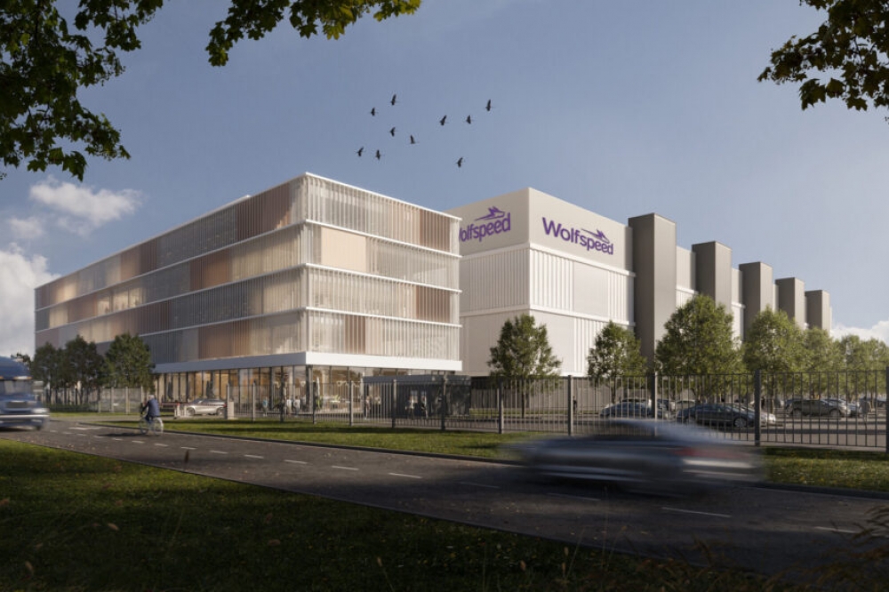
Wolfspeed has announced plans to build a highly-automated, cutting-edge 200mm wafer fabrication facility in Saarland, Germany.
The company says its first fab in Europe will be its most advanced, creating a breakthrough innovation SiC development and production facility in the European Union to support growing demand for a wide variety of automotive, industrial and energy applications.
The Wolfspeed facility is planned as part of a collaboration within the IPCEI for Microelectronics and Communication Technologies framework, and is dependent upon state aid approval from the European Commission. IPCEI funding is intended to support technology development and initial deployment within this project. ZF Friedrichshafen also intends to support the new construction by making a sizeable financial investment as part of a new strategic partnership announced separately.
The European fab announcement is part of the company’s broader $6.5 billion capacity expansion effort, which includes opening of the company’s 200mm Mohawk Valley device fab in April 2022, and the construction of The John Palmour Manufacturing Center for SiC, a 445-acre (180 hectare) SiC materials facility in North Carolina, which will expand the company’s existing materials capacity by more than 10x. The first phase of construction for the materials facility is slated to be complete by the end of FY2024.
“This new fab represents a big step forward for both Wolfspeed and our regional customers, as we enhance the ecosystem for semiconductor production and innovation,” said Gregg Lowe, president and CEO of Wolfspeed. “SiC devices offer greater energy efficiency and are essential in the global shift toward sustainable electrification. This new facility will be crucial to supporting our expansion in a capacity constrained industry that is growing very rapidly, especially across the EV marketplace. It was important for us to have a facility located in the heart of Europe, near many of our customers and partners, to foster collaboration on the next generation of SiC technologies.”
The announcement was made at an event on the 35-acre (14-hectare) site of the planned fab, a former coal-fired power plant in Saarland, Germany. German Chancellor Olaf Scholz was in attendance to welcome Wolfspeed to the region, as well as Robert Habeck, Vice Chancellor of Germany and Federal Minister for Economic Affairs and Climate Action, and Saarland Minister-President Anke Rehlinger.
Representing the new partnership, ZF CEO Holger Klein, and Stephan von Schuckmann, Member of the ZF Board of Management also joined in the announcement. Wolfspeed also announced today a strategic partnership with ZF that includes an investment in Wolfspeed as well as a joint SiC R&D facility in Germany, which is part of the same IPCEI framework. Fab construction is anticipated to begin in the first half of 2023, subject to approval by the EU Commission.
“This project is a great transformation driver and a job engine for a traditionally industrial region. Furthermore, it bundles important know-how in Europe and contributes to the implementation of the European Green Deal by reducing energy consumption and CO2 emissions,” said Saarland Minister-President, Anke Rehlinger. “We’re proud to have Wolfspeed, and have our region play such a vital role in advancing SiC semiconductor innovation.”
The fab will employ more than 600 people when fully operational.
The adoption of SiC power devices is rapidly growing across multiple markets, including renewable energy and energy storage, electric vehicles, charging infrastructure, industrial power supplies, traction and variable speed drives. SiC enables smaller, lighter and more cost-effective designs, converting energy more efficiently to enable countless new clean energy applications.


