
Advancing quantum photonics with transfer printing
Transfer printing produces CMOS-compatible integration of a silicon platform with quantum-dot single-photon sources
A collaboration between researchers in Japan and Germany is claiming to have broken new ground in the integration of single-photon sources and silicon photonic integrated circuits. According to the team, they are the first to unveil hybrid integration of quantum-dot single-photon sources in the telecom band with silicon photonic integrated circuits made in silicon foundries.
This advance by engineers from a number of institutions – Toyohashi University of Technology, The University of Tokyo, Keio University, The University of Electro-Communications and the University of Kassel – promises to aid the construction of large-scale quantum photonic integrated circuits. Such circuits could be used for quantum simulation, quantum communication and quantum machine learning.
Options for providing single-photon sources for quantum circuits include III-V quantum dots, colour centres in diamond and SiC, and defects in two-dimensional materials. Of these, there’s much merit in InAs/InP quantum dots, according to team spokesman Ryota Katsumi, who is affiliated to Toyohashi University of Technology and The University of Tokyo.
Katsumi told Compound Semiconductor that quantum dots are ideal for meeting the requirements for single-photon sources, which include bright single-photon emission, high purity, deterministic operation and high indistinguishability. “It is difficult for other single-photon sources to perform all of these requirements at once.”
The team’s latest triumph builds on previous successes, including using transfer printing to realise the hybrid integration of InAs/GaAs quantum-dot single-photon sources on a CMOS-processed chip.
For that work, the sources produced emission outside conventional communication bands. By now moving to the O and L bands via the switch from dots on GaAs to those on InP, the researchers are benefitting from low loss and low dispersion propagation through optical fibre – this is advantageous for long distance and secure quantum networks.
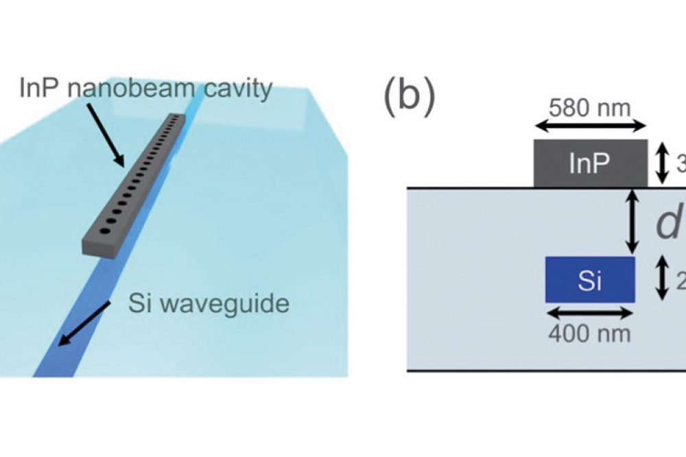
The latest work began with the growth of InAs quantum dots on an InP substrate via MBE. Using the addition of a hard mask, electron-beam lithography and dry and wet etch etching, photonic-crystal nanobeam cavities were formed from the epiwafers. Transfer printing re-located this structure to a silicon waveguide cladded with glass (see Figure).
Micro-photoluminescence measurements at 13 K, using optical excitation from a 785 nm laser, produced a strong quantum-dot emission peak at 1436.9 nm and a fundamental cavity mode at 1436.2 nm. The single-photon coupling efficiency from the dots to the waveguide is 82 percent.
In the nanobeam cavities produced by the team around 10 quantum dots couple to the cavity. Some of these dots are outside the cavity’s resonance, leading to background emission and a degradation of a key figure of merit known as g(2), which is a measure of the degree of second-order coherence.
“For purer single-photon emission, it is necessary to employ a single quantum dot,” remarked Katsumi, who added that an attractive way to realise this is to produce epiwafers with a much lower quantum-dot density.
As well as improved purity of emission, integrated quantum photonic circuits need single-photon sources that are electrically driven, rather than optically pumped. According to Katsumi, the team’s technology offers a way to do this. “Transfer printing could even be used for the implementation of the electrodes for electrical pumping on silicon.”
To realise practical quantum photonic information processing, there needs to be efficient, plug-and-play coupling between single photons and fibre – this will ensure long-distance quantum networks.
Katsumi and co-workers are targeting this, with efforts directed at making modularize solid-state single-photon sources by transfer printing. “This will enable the efficient and stable supply of single photons for future quantum applications.”
Reference
R. Katsumi et al. Appl. Phys. Express 16 012204 (2023)


