
From sheets to stacks
Tunnel FETs realised with multi-layered in-plane transition metal dichalcogenide junctions
Scientists from Tokyo Metropolitan University have successfully engineered multi-layered nanostructures of transition metal dichalcogenides (TDMCs) which meet in-plane to form junctions.
They grew out layers of multi-layered structures of MoS2 from the edge of niobium doped MoS2 shards, creating a thick, bonded, planar heterostructure. They demonstrated that these may be used to make new tunnel field-effect transistors (TFET), for use in integrated circuits with ultra-low power consumption.
While MOSFETs form the majority of FETs in use today, the search is on for the next generation of materials to drive increasingly demanding and compact devices using less power. This is where tunneling FETs (or TFETs) come in.
TFETs rely on quantum tunneling, an effect where electrons are able to pass usually impassable barriers due to quantum mechanical effects. Though TFETs use much less energy and have long been proposed as a promising alternative to traditional FETs, scientists are yet to come up with a way of implementing the technology in a scalable form.
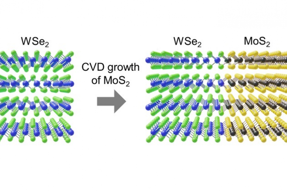
In this latest work, the scientists from Tokyo Metropolitan University led by Yasumitsu Miyata, showed that by using a CVD technique, they could grow out a different TMDC from the edge of stacked crystalline planes mounted on a substrate. The result was an in-plane junction that was multiple-layers thick.
Much of the existing work on TMDC junctions use monolayers stacked on top of each other; this is because, despite the superb theoretical performance of in-plane junctions, previous attempts could not realise the high hole and electron concentrations required to make a TFET work.
After demonstrating the robustness of their technique using MoS2 grown from WSe2, they turned their attention to niobium doped MoS2, a p-type semiconductor. By growing out multi-layered structures of undoped MoS2, an n-type semiconductor, the team realised a thick p-n junction between TMDCs with unprecedentedly high carrier concentration.
Furthermore, they found that the junction showed a trend of negative differential resistance (NDR), where increases in voltage lead to less and less increased current, a key feature of tunneling and a significant first step for these nanomaterials to make their way into TFETs.
The method employed by the team is also scalable over large areas, making it suitable for implementation during circuit fabrication.
Reference
'Multilayer In-Plane Heterostructures Based on Transition Metal Dichalcogenides for Advanced Electronics' by Hiroto Ogura et al; ACS Nano 27 Feb 2023


