
Cardiff researchers re-shape quantum dots
From cubes to complex truncated octahedra, researchers say nanocrystals have unique optical and electronic properties
A Cardiff University-led team has developed a new method of controlling the shape of quantum dots, providing new ways to optimise optoelectronics, energy harvesting, photonics, and biomedical imaging technologies.
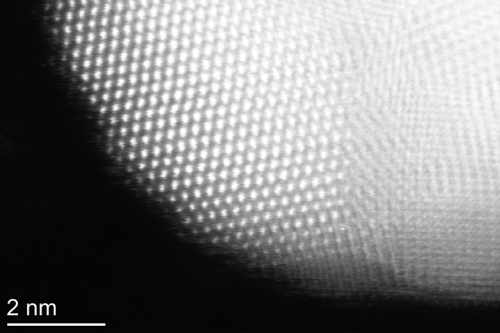
The study, funded by the Engineering and Physical Science Research Council (EPSRC) and published in Nano Letters, used nanofaceting – the formation of small, flat surfaces on nanoparticles – to manipulate the quantum dots into a variety of nanocrystals.
From cubes and olive-like structures to complex truncated octahedra, the international team of researchers say these nanocrystals have unique optical and electronic properties, which can be used in different types of technology.
Bo Hou, a senior lecturer at Cardiff University’s School of Physics and Astronomy who led the study, said: “Quantum dots have the potential to revolutionise a number of industries because of the theoretically limitless efficiencies they offer. Our study is a significant step forward in the adoption of quantum dots technology across a wide range of energy and lighting industry applications.
“With further development, we might imagine the truncated octahedra we manufactured being used for energy harvesting in solar cells, improving efficiencies beyond the capabilities of current technologies which sit at around 33 percent. Likewise, our nanocrystals might be used for biomedical imaging, where inefficiencies and instabilities are currently limiting their use in diagnoses and drug delivery.
“So, these technologies really are the future and for our work to play a part in accelerating their application is really exciting.”
Working out of Cardiff University’s new Translational Research Hub (TRH), the team grew the compound semiconductor nanocrystals in solvent and monitored their development in real time using computer simulations and powerful microscope technology.
Hou added: “Growing the semiconductors in solvent was our preferred choice because of its low carbon footprint, potential for higher yield and economic benefits when compared to the high temperatures and vacuum conditions needed in traditional production.
“It also meant we were able to study the effect of solvent polarity on the shape of the nanocrystals, which could provide a means to stabilise polar surfaces with further research.”
The team is now developing image sensors and low-carbon footprint LEDs which will enable industry to implement the quantum dot nanocrystals into their technologies to boost their resolution and energy efficiency.


