£1B UK strategy focuses on compound semis

UK government announces 20-year plan to secure UK's semiconductor strengths
The UK's long awaited National Semiconductor Strategy sets out how up to £1 billion of government investment will boost the UK’s strengths and skills in design, R&D and compound semiconductors, while helping to grow domestic chip firms across the UK.
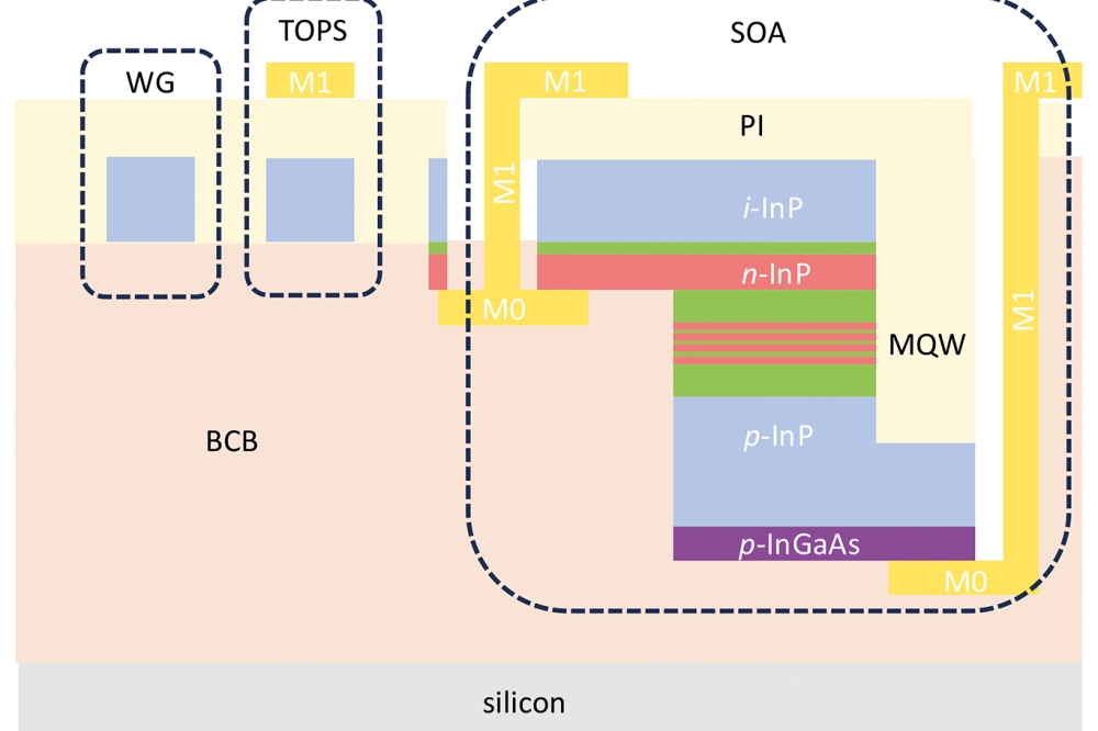
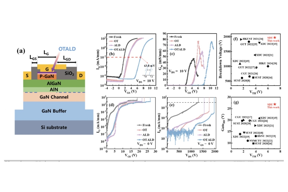
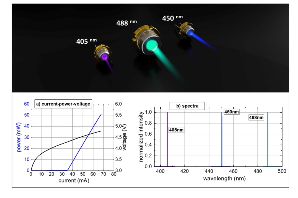
The strategy focuses on the UK’s strengths – semiconductor design, compound semiconductors, and the R&D ecosystem - supported by UK universities from Cambridge to Cardiff and Manchester to Edinburgh.
To support the growth of the compound semiconductor sector in the UK, the government will invest up to £200 million over the next two years, and up to £1 billion in the next decade.
The aim is to improve industry access to infrastructure, power more research and development and facilitate greater international cooperation. Funding will also be used to improve the talent pipeline and will make it easier for British firms to access things like prototyping, tools and business support.
The UK’s Integrated Review placed securing strategic advantage in science and technology at the heart of the UK’s national security and foreign policy. In recognition of the fundamental importance of semiconductor technologies in these areas, the National Semiconductor Strategy demonstrates a clear vision for the UK's position in the sector.
As part of the strategy, the UK will increase its cooperation with close partners, working together to manage national security threats and driving growth in the sector, while championing international cooperation to help develop a coordinated approach to supply chain resilience.
In Hiroshima last week,, the UK and Japan committed to establishing a semiconductor partnership, led by the UK’s Department for Science, Innovation and Technology (DSIT) and Japan’s Ministry of Economy, Trade and Industry (METI). It seeks to deliver new R&D cooperation, skills exchanges, and improving the resilience of the semiconductor supply chain for both countries.
UK Research and Innovation will work with the Japan Science and Technology Agency on a joint investment of up to £2 million in early stage semiconductor research next year. This will support UK and Japanese researchers to work together on fundamental semiconductor technologies.
The strategy has been developed in close consultation with the semiconductor industry and academia, and the government will build on this partnership by creating a new UK Semiconductor Advisory Panel. The Panel will bring together key figures from industry, government, and academia to work closely on shared solutions and implementation.
These efforts will include investment in a new National Semiconductor Infrastructure Initiative to unlock the potential of British chip firms in these key areas. It will look at whether better access to prototyping facilities for chip firms is needed to tackle barriers to innovation and grow the industry. It will also explore opportunities to make specialist software tools more available for start-ups.
The government will announce plans by the autumn on support for investment in the semiconductor manufacturing sector, particularly where they are critical to the UK tech ecosystem or the UK’s national security.
Americo Lemos, CEO of UK compound semiconductor wafer firm IQE plc, said: "The Semiconductor Strategy rightly focuses on the areas where the UK is a global leader, such as the manufacturing of advanced compound semiconductors sitting at the heart of future technologies.
"With significant investment now being allocated to semiconductor manufacturing in places like the US, Europe and Asia, there’s no time to lose in bolstering the UK’s capabilities. We’re excited to work closely with the government to implement this Strategy quickly and help realise the UK’s true potential."


