
New home for the Institute for Compound Semiconductors
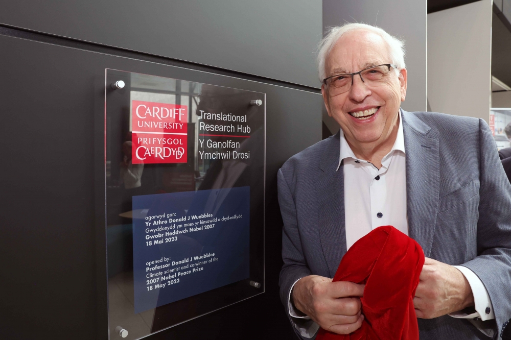
Nobel-prize-winning climate scientist Donald Wuebbles opens Cardiff University’s Translational Research Hub, a new home for the Institute for Compound Semiconductors.
BY RICHARD STEVENSON, EDITOR, CS MAGAZINE
One the cornerstones of the world’s first compound semiconductor cluster, situated in South Wales, is the Institute for Compound Semiconductors (ICS). Launched in 2015, the long-term plans for this driver of device development have always included a move to a new, purpose-built facility with the capability to process wafers up to 200 mm in diameter. Now finally – and to the immense relief of some of those involved – this has been accomplished, with the new facility up and running and open for business.

On-wafer measurements
of VCSELs and edge-emitting lasers are undertaken at the ICS.
To mark this key milestone in the life of the ICS, which is part of Cardiff University, this institute held an official opening on Thursday 18 May. At that celebration for what is now the largest building on the Cardiff Innovation Campus, and the new home to both the ICS and Cardiff Catalysis Institute – together they form what is known as the Translational Research Hub – Nobel-prize-winning climate scientist Professor Donald Wuebbles unveiled a plaque to mark the occasion. He also delivered one of a number of talks that formed the centrepiece of this joyous occasion, showcasing the new capabilities of the ICS.
Those that spoke included Cardiff University’s Pro Vice Chancellor Professor Rudolf Alleman, who discussed the many challenges associated with the construction of the Translational Research Hub, which is located on a site previously occupied by railway sidings. Initially the ICS was slated to be up and running in its new home in 2020, but who could have foreseen the problems caused by the Covid pandemic, or material supply issues associated with Brexit.
A reminder of the motivation for forming the ICS came from its Managing Director, Professor Peter Smowton. He explained that the vision for the facility, which is a resource that academia and UK industry are able to use, came together in 2013 to address what he describes as ‘the valley of death’. This phrase relates to the pitfalls that arise when trying to take a promising device technology from the fab and use it to establish a successful, high-volume product.

There is tremendous expertise in high-frequency measurements at the ICS.
Smowton is well versed in the challenges of taking a bespoke device with champion results and building on this to create a high-performance, high reliability commercial product. His solution, adopted by the ICS, is that fundamental device development is undertaken with fab tools that are suitable for high-volume manufacture.
Aiding commercialisation of device development is not the only benefit of this approach, however, argues Smowton. He points out that at the heart of the research of many academics is the testing of a hypothesis, which hinges on being able to employ repeatable processes. So pure research also benefits from the highly capable, high-volume tools in the ICS, because they speed the drawing of conclusions from experimental work, as well as the level of rigour.

The Translational Research Hub, the new home for the Institute for Compound Semiconductors (ICS), features 4,350 m2 of labs, including cleanroom, and 1,750 m2 of offices.
A diverse research portfolio
During the official opening of the ICS, this institute showcased its diversified research programme, with brief talks given by a number of academics.
Dr Naresh Gunasekar, a member of the ICS that holds a lectureship position within the Condensed Matter and Photonics Group in the School of Physics and Astronomy, explained that one of his interests relates to the manufacture of wide bandgap semiconductors. His group is concerned with the efficiency of these devices, as well as testing their reliability.
Another researcher sharing their focus, Professor Khaled Elgaid from the ICS and Cardiff University’s School of Engineering, spoke about the consequences of energy consumption arising from the shift from 4G to 5G. This evolution will lead to 100 billion connected devices. Armed with tremendous expertise in high-frequency transistors based on a variety of III-Vs, he is involved in the development of GaN HEMTs that are hoped to deliver a step-change in performance.
The ICS also develops sensors for healthcare. Arathy Varghese briefly discussed efforts at developing devices based on the GaN HEMT that could detect cancers and provide personalised healthcare in homes.
Attendees at the official opening of the Translational Research Hub were also given a tour of the premises. This included a visit to the lab that provides high-frequency measurements of III-V devices, where the current focus is on investigating the characteristics of GaN RF devices. This lab has expertise in measuring very high frequencies, and identifying driving conditions that match harmonics to enable exceptional efficiencies.
Visitors were also taken to a lab that provides on-wafer optical characterisation of light-emitting devices. As well as characterising VCSELs, this group has developed techniques to investigate the performance of edge-emitters, by etching into the epiwafer.
In addition to the capability to measure devices, the ICS is able to make them. There’s an MBE reactor within the university, and ICS partners with IQE for epiwafers produced by MOCVD, which can be grown at the company’s St Mellon’s facility that is now focusing on development runs.
Processing of devices into epiwafers takes place in the cleanrooms at the ICS. The institute has an extensive range of tools, with the capability to define structures, deposit contacts and add passivation materials, including via atomic layer deposition. Dimensions, defined by photolithography, could soon be extended to the nanometre scale, thanks to the delivery of an electron-beam tool.
It’s clear that the move into this well-designed and equipped building is enthusing those working at there. The have waited a long time – but it’s been worth it.


