

Photovoltaics: Towards 50 percent efficiency
A record-breaking photovoltaic efficiency comes from bonding a pair of
dual-junction solar cells with different lattice constants.
BY OLIVER HÖHN FROM FRAUNHOFER ISE
What's needed to realise exceptionally high efficiencies with solar cells? A significant degree of concentration is a given, alongside the use of multi-junction solar cells, with history attesting that the best results tend to come when these devices are produced by MOCVD. Allied to these key attributes, the fabrication of best-in-class devices demands great designs, excellent expertise, and thorough process technology.
The success story of multi-junction solar cells begins decades ago, with the deployment of these devices in space. Satellites have been powered by solar cells for many years, and for this application a high efficiency is incredibly valuable. Due to this, III-V multi-junction solar cells have had a stranglehold on this market since the 1990s, when they replaced their silicon siblings. Since then efficiencies have increased, but the standard product for space applications is still the triple-junction solar cell, produced on a germanium substrate that also provides the lowest sub-cell.
To bring this technology from space to earth, it is essential that the expensive III-V solar cell is used far more effectively. This can be accomplished by placing high-efficiency, multi-junction III-V cells in concentrating photovoltaic (CPV) systems. In this case, the expensive large-area semiconductor is replaced by a lens, which focuses sunlight onto a very small solar cell, thereby reducing the size of the III-V material that’s required by a factor of 500-1000, depending on the concentration of the lenses.
The benefits of concentration are not limited to slashing the outlay on multi-junction cells. In addition, the increase in concentration enhances the efficiency of the solar cells by a thermodynamic effect. The increase in current density leads to a logarithmic increase in voltage – this is a fundamental consequence of diode characteristics – and as the power that’s generated by the solar cell is the product of its voltage and current, there is an increase in efficiency under concentration.
Over the past ten years or so, efforts to increase solar cell efficiency have included the introduction of more junctions, with devices featuring up to six of them. Efforts in this direction highlight the limitations of this approach, with monolithic epitaxial growth requiring lattice-matching of an increasing number of sub-cells, each made from III-Vs differing in content or composition. This requirement restricts the range of band gaps that can be employed within one monolithic device.
In general, two approaches have been pursued to overcome this limitation. One option, arguably the less radical of the two, is to introduce metamorphic buffers that gradually change the lattice constant, thus opening the door to a broader range of band gaps. However, there’s a penalty to pay for grading the lattice constant: material quality suffers, dragging down solar cell performance.
At Fraunhofer ISE, our team adopted a different approach. In our case, we grow lattice-matched top junctions with high band gaps on a GaAs substrate; and we use an InP substrate for lattice-matched growth of the bottom junctions, which have lower band gaps (see Figure 1). These two devices, which have totally different lattice constants, are monolithically stacked on one another, using surface-activated direct wafer bonding. By taking this approach, we overcome the limitations in cell performance that stem from a metamorphic buffer.
Over the last few years we have engaged in friendly competition with a team at NREL for the world record in solar cell efficiency. Back in 2015 we gained the lead, in partnership with Soitec and CEA, with a wafer-bonded four-junction solar cell with an efficiency of 46 percent. We held the record until 2019, when NREL reported a metamorphic six-junction device with an efficiency of 47.1 percent. Then last year we announced that we had improved on this value, realising a record for photovoltaic efficiency of 47.6 percent, through a BMWK-funded project entitled ‘50 Prozent’ (03EE1060).
While regaining the record is a triumph in itself, we are particularly pleased that we have accomplished this with a device with just four junctions. We attribute this success to the game-changing direct wafer bond, allied to the excellent design and realisation of a pair of dual-junction lattice-matched ternary and quaternary solar cells on InP and GaAs. We shall soon detail the magic of the wafer bond, but before we get to that, we’ll discuss the cell design in more detail.

Figure 1. (Left) The two lattice-matched tandem devices, grown on GaAs
and InP, use several different alloys to form the sub-cells. High band
gap materials GaInP and AlGaAs are lattice-matched to the GaAs growth
substrate, and low band gap sub-cells made from GaInAsP and GaInAs are
epitaxially grown on InP. (Right) The process flow for a wafer-bonded
four-junction solar cell. After epitaxial growth of two tandem cells on
their respective growth substrate, surfaces are cleaned and polished
again, activated with an ion beam and then bonded with a direct wafer
bonder. Afterwards contacts and an anti-reflection coating are added
with microfabrication steps.
Current matching
The starting point for fabricating any highly efficient multi-junction solar cell is an optimised optical and electrical design. In monolithic solar cells, sub-cells are connected in series by so-called tunnel diodes, so it is imperative to carefully match the current generation of these sub-cells, and thus their absorption. While it is possible to optimise the electrical design of each sub-cell independently, carefully selecting values for the likes of the emitter thickness and doping, it is crucial to optimise the optical design for the entire device. Due to this, designers of multi-junction cells tend to use optical modelling tools, such as a transfer matrix algorithm, to determine the exact sub-cell band gaps and thicknesses for the entire device, which will contain tens of layers.
A great design, in itself, is no guarantee of success. What’s needed is to transfer this into working devices in a perfect manner. Consequently, the only way to realise solar cells with efficiencies approaching 50 percent is for them to behave exactly as designed.
We have taken major strides in this direction, developing a strategy that links modelling and realisation so accurately that it enables a perfect current match for a four-junction solar cell. Thanks to this advancement, success stems on ensuring a high-quality direct wafer bond between the MOCVD-grown dual-junction bottom cell on InP, and the inverted dual-junction top cell on GaAs, which includes the tunnel diodes and the bonding layers.
Wafer bonding
The idea behind direct wafer bonding is the adhesive-free joining of two flat surfaces, realised by simply bringing them into contact with one another. This should result in one single device with a chemical bond at the interface that is as strong as the bulk materials. With this technique almost any pair of materials can be joined, including crystals with different lattice constants. Consequently, there are many options for direct wafer bonding within the semiconductor industry.
To establish atomically flat surfaces, technicians can turn to chemical-mechanical polishing, which is a combination of mechanical polishing and chemical etching. This is a standard treatment during the fabrication of wafers for the semiconductor industry, because such perfect surfaces are essential for many process steps, including epitaxial growth. If necessary, the surface can be cleaned and polished again before direct wafer bonding, in order to improve bond quality and yield.
In our case, we use direct wafer bonding to join two dual-junction solar cells. Both contain many layers with differing compositions, and are capped with a highly doped bonding layer. We optimise this layer to ensure a good electrical contact of the sub-cells. To that end, we can thin it down with an extremely defined and homogeneous chemical mechanical polish to remove any defects and produce a perfectly smooth surface. We used here the expertise of III-V Reclaim to optimize the processes depending on the compound semiconductor used and its surface roughness. After this polishing step, we place the wafers inside the bonding chamber (see Figure 2). The surface is then activated by a fast ion beam that removes residuals, such as oxides, from the surface – this is also known as sputter etching. An ultra-high vacuum preserves the dangling bonds of the activated surface atoms. That enables chemical bonding, even at room temperature, when the wafers are pressed together. During this step an amorphous layer forms at the interface – it is optically inactive but electrically conductive, due to a thickness of only a few nanometres. A final annealing step delivers additional improvement to the mechanical strength and the electrical contact. That’s all the magic.

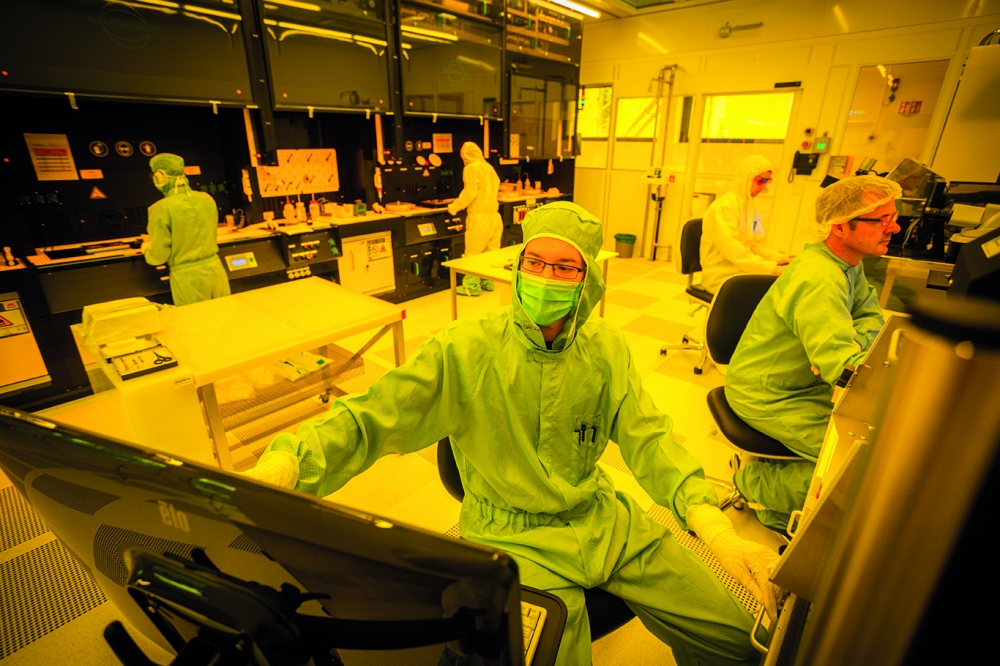
Figure 2. In front of the direct wafer bonder are: technician Rita
Freitas, who fabricates wafer-bonded four-junction wafers into solar
cells; and Oliver Höhn, head of the group III-V semiconductor
technology, and project manager of the BMWK funded project “50Prozent”.
The bonding chamber includes ion sources for surface activation and
chucks for the substrates to be bonded.
Note that while our use of direct wafer bonding for the fabrication of solar cells is novel, the technique itself is tried and tested. It’s been known for decades, and has become popular in recent times, where it has found increasing application in the production of micro-electro-mechanical systems and ICs. In some fields, direct wafer bonding has already found its way to high-volume manufacturing. There is a growing interest in this technique, due to its manifold applicabilities, as well as the availability of fully-automated high-throughput tools for production lines.
Precision fabrication
After wafer bonding of the device, we remove the GaAs substrate with a wet-chemical step that creates a monolithic four-junction structure on an InP substrate. We transform this structure into a working solar cell with microfabrication steps that include photolithography, wet-chemical etching, and evaporation.
We take steps to minimise optical losses, which can come from reflection at the front interface and shading losses from fingers. To this end we have developed a specially designed anti-reflective coating that consists of alternating layers of MgF and TiO2. Applying this coating, which we refer to as four-layer Herpin, ensures the lowest possible reflectance over the broad acceptance range of the solar cell. The fingers that we employ are specially shaped to have a trapezoidal cross section, leading to a significant decrease in shading losses, as light hitting the fingers is partially reflected towards the solar cell, where it contributes to current generation.
Measurements on this device in our Callab reveal an efficiency of 47.6 percent at a concentration of 665 suns.

Figure 3. External quantum efficiency (EQE) and current-voltage (I-V)
characteristics of the record wafer-bonded four-junction solar cell. The
EQE measurement reveals excellent current matching of the four
sub-cells.
Towards 50 percent
Our roadmap to even higher efficiencies includes the introduction of a next-generation design that we are calling the rear hetero-junction solar cell. This device will feature optimised contact fingers that redirect even more light into the solar cell to decrease shading losses. We also plan to increase the number of junctions to six. With all these advances, we anticipate that we will smash the 50 percent barrier.
While this is an important milestone that will highlight the potential of CPV technology, this class of photovoltaic will only be able to compete with silicon PV if there’s a fall in costs. Thus, one of our short-term targets is to slash the cost of III-V solar cells. Helping to accomplish this goal is: the implementation of techniques from large-scale silicon technology, such as screen-printed contact fingers; re-use of the substrate; and the introduction of low-cost epitaxy.
Our overarching goal, shared by our industry partners, is to develop a cost-competitive, high efficiency III-V-based solar device that can serve in various earth and space applications, and be integrated into the likes of vehicles and aircraft. The 50 percent cell is an important milestone and a lighthouse. However, it is not yet clear whether commercial success will come from our wafer-bonded cell, or a simpler device based on our findings. Time will tell.


